After the VT52 has been installed and checked out at the customer’s site, it can be expected to operate
error free for long periods of time. As with all electronic devices, however, the VT52 will occasionally
require some corrective maintenance due to a failing or marginal component. When the terminal
requires service, it is recommended that service be performed at the subassembly level; the fault should
be isolated to a module or other major component and the faulty part replaced with a completely
tested spare. If the failing part is a module, it should be returned to an authorized DIGITAL repair
depot where facilities are available for efficiently locating the faulty component. After repair and
complete testing, the module can be returned to Field Service stock.
With the exception of the Monitor/Power Supply module, all data and control circuitry in the VT52
depends upon the microprocessor for timing and/or data information. Without specially designed test
equipment, field testing this circuitry to the component level is difficult and time consuming and is not
recommended.
NOTE The spares kit consists of a complete set of modules for the VT52.
5.2 Subassembly Level Troubleshooting
To find and repair the cause of a failing terminal, the serviceman must first identify the faulty subassembly
and then replace it with a good spare part. Replacement procedures for all major subassemblies
are described in Paragraph 5.3. To identify the faulty subassembly, the serviceman must
analyze the symptoms and make a judgment as to which module or major component is at fault.
Replacing the suspect subassembly will fix the problem or at least eliminate that subassembly as a
possible cause of the problem.
5.2.1 Identifying the Faulty Subassembly
Identifying the faulty subassembly will be fairly easy in some cases and quite difficult in others. Failures
to the Monitor/Power Supply module will usually result in an obvious display malfunction, i.e.,
loss of horizontal or vertical deflection, no display, etc.
In some cases, the serviceman will be able to decide which subassembly is failing by analyzing the
symptoms displayed on the screen. In other cases he will have to make additional keyboard tests
and/or voltage and waveform checks to determine the failing subassembly. To assist you in making
this decision, timing waveforms and other test data are included in this chapter.
The PMK04 Off-Line Terminal Tester can be used to exercise serial terminals and assist the serviceman
in isolating faults within the terminal or communications interface. (Refer to PMK04 manual).
5.2.2 Analyzing the Symptoms
To start with there are some basic checks the serviceman should make before disassembling the unit.
Is the unit turned on?
Is the unit plugged into the outlet?
Is the intensity level set too low?
Are the baud rate switches set to legal positions?
Are the send/receive baud rates of the terminal set to the receive/send baud rates of the
host?
After determining that the terminal is properly set up for operation and still does not work, the unit
should be placed off-line and some keyboard tests made to develop a list of symptoms and possible
causes. The more symptoms the serviceman has to work with, the better the judgment that can be
made as to which part is failing.
NOTE The possible equipment malfunctions listed in Tables
5-1 and 5-2 are categorized by abnormal symptoms.
Corresponding causes are listed in order of probability.
Corrective actions are for the most part limited
to the adjustment and/or substitution of major replaceable
subassemblies.
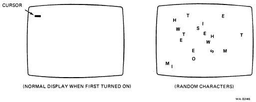
After warm-up, is the cursor at HOME position and blinking?
If not, go to step 2.
If the cursor is at HOME position, the serviceman can assume that the CRT and its associated
components and the Monitor/Power Supply module are all functioning normally. Further
testing is required (Table 5-2).
Is there a raster on the screen when the intensity level is set for maximum brightness?*
* On some units the raster is not visible even with the intensity control set for maximum brightness.
If there is no raster, see Table 5-1.
If there is a raster, the serviceman can assume that the MONITOR/PS module and the CRT
and its associated components are alright. A possible exception is the video amplifier circuitry
on the Monitor/PS module.
If further testing is required to locate the problem, the unit must be tipped back and the base removed.
The base removal procedures are described in Paragraph 5.3.
Table 5-1 Power On Troubleshooting Procedure
Symptom
Possible Cause
Corrective Action
No cursor
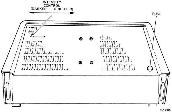
Intensity control turned down
Adjust intensity control (Figure 5-1)
No cursor, raster missing
Blown fuse
Replace fuse (Figure 5-1)
Figure 5-1 Intensity Control and Fuse Locations
No cursor, raster missing
No prime power
Restore source of prime power
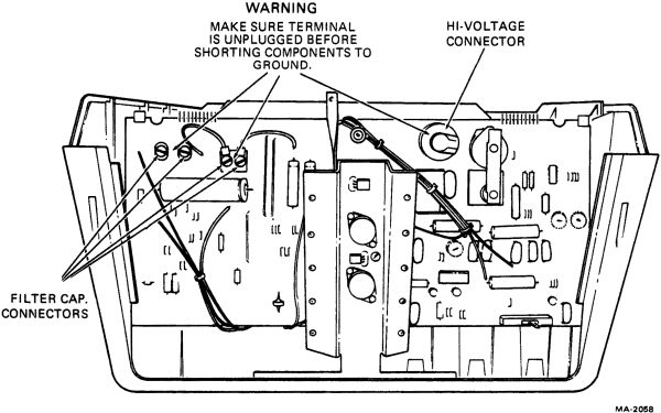
WARNING
There are high voltages present in the power supply
and CRT. Make sure the terminal power line is unplugged
and the CRT and capacitors are discharged
as shown in Figure 5-2 before handling the power
supply or CRT components. Make sure ground connection
is made before discharging these points.
WARNING
There are high voltages present in the power supply
and CRT. Make sure the terminal power line is unplugged
and the CRT and capacitors are discharged
as shown in Figure 5-2 before handling the power
supply or CRT components.
Raster too large; all characters enlarged and fuzzy (Figure 5-12)
Incorrect yoke position
Push yoke forward to the CRT bell as far as it will go. Tighten hold down screw.
Figure 5-12 Enlarged and Fuzzy Characters Indication
5.3 Subassembly Replacement
The following paragraphs provide step-by-step procedures for swapping modules and major components
in the VT52 terminal.
5.3.1 Removing the Base Assembly
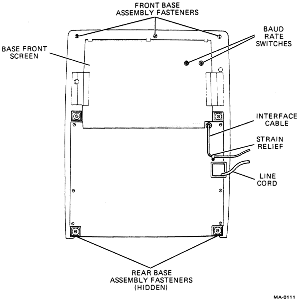
To remove the base assembly refer to Figure 5-13 and perform the following steps.
Make certain the unit is not plugged into an electrical outlet and the power (ON/OFF)
switch is OFF.
Place the unit upside down on a bench or table.
Unscrew the sliding cover (two screws) covering the line cord opening.
Remove the base front screen (three screws).
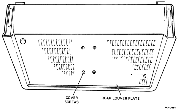
Remove the screws (as many as ten) holding the rear louver plate on (Figure 5-15).
Remove ground leads.
Slide the interface cable and its rubber grommet from the slot in the rear screen.
Unfasten the ground connection from the rear of the base screen (one screw).
Remove the base assembly from the shell by first turning the five, ¼ turn fasteners 90°
counterclockwise. Notice that the five ¼ turn fasteners are not removed but merely turned,
using a ¼ inch nut driver, 90° counterclockwise to loosen, and 90° clockwise to tighten.
Reverse steps 1 through 9 to reassemble.
To remove the base assembly from older units,* do steps 1, 2, 3, and 4. Then remove the base-securing
screws with a ¼ inch nut driver and lift the base from the unit.
* Up to and including the following serial numbers: Westfield serial number 3657, Phoenix serial number 5400.
Figure 5-13 Base Assembly Removal and Replacement
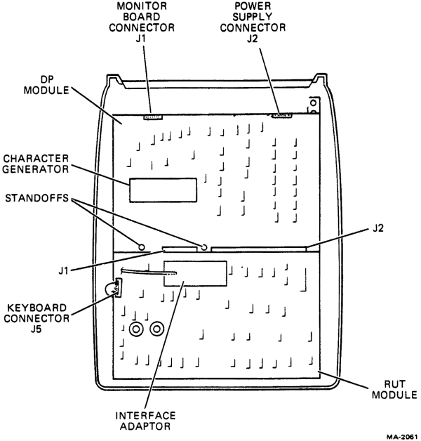
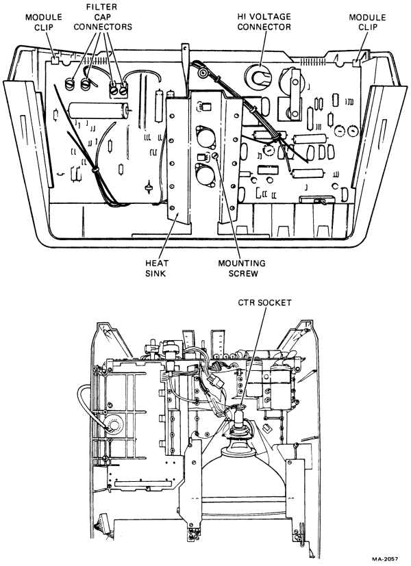
Figure 5-14 is a bottom view of the terminal with the base cover removed. J1 and J2 on the ROM,
UART, and Timing (RUT) module connect directly to J1 and J2 on the Data Path, Memory, and
Decoder (DP) module. The keyboard is cable connected to RUT connector J5. The Monitor signals
are cable connected to DP-J8; the Power Supply is cable connected to DP-J9.
Figure 5-14 RUT and DP Module Removal and Replacement
5.3.2 Replacing the ROM, UART and Timing (RUT) or Data Path, Memory
and Decoder (DP) Module
The RUT module and the DP module must be removed and replaced as a unit; they should not be
separated until they have been removed from the terminal. To replace the RUT/DP modules, refer to
Figure 5-14 and do the following:
Unplug the EIA or 20 mA adapter card, the keyboard connector, and the two connectors to
the power supply board.
Unscrew nine small plastic wing nuts.
Remove two 8-32 × ¼ inch aluminum standoffs.
Pick up the assembled board set from the unit and set aside. Separate the RUT module from
the DP module being careful to save the small plastic clip holding the corners of the two
boards.
A board set must be reassembled (including the small plastic clip) outside the shell and
installed as a set. It is installed by sliding the front board slots under the three front ¼ turn
fasteners and over the 8-32 studs.
The plastic wing nuts can be screwed on or pushed on with a smaller nut driver.
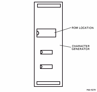
If the character generator is to be removed from the DP module, unplug the assembly. (The
character generator is secured to the DP module by its connectors).
To replace the RUT and DP modules reverse steps 1-8.
The following steps outline the procedure to be followed when removing the RUT or DP module from
earlier terminals (Westfield serial number 3657 and lower; Phoenix serial number 5400 and lower).
CAUTION
When replacing the RUT and DP modules, make
sure that connectors are aligned properly before applying
pressure. Observe that color-coded wires on
both sides of the connectors match and, where indicated,
pin 1 is located at the extreme left of the
connector as shown in Figure 5-14. If the character
generator has been removed, make sure the arrow on
the assembly points to the rear of the unit.
5.3.3 Replacing the Monitor/Power Supply Module
WARNING
There are high voltages present in the power supply.
Make sure that the terminal line cord is not plugged
into a source of power when servicing, removing, or
replacing power supply assemblies or components.
Using a screwdriver or clip lead, discharge the filter
capacitors by shorting the capacitors to the assembly
chassis or any suitable ground. Make sure ground
connection is made before discharging the
capacitors.
Remove screws (as many as ten) holding the heat sink (louver plate) plate on. Set heat sink
aside.
Remove ground leads.
Disconnect 9-pin Mate-N-Lok connector.
Disconnect the socket from the neck of the CRT and the Faston connector on the black
ground wire from the braided strap.
Disconnect the 6-pin Mate-N-Lok that connects the yoke to the Monitor/Power Supply
board.
Disconnect the four wires from the two large capacitors. Note that the red wires go to the
positive terminal.
Remove the two small plastic clips holding the left and right corners of the power supply
board.
Remove one screw from the middle of the heat spreader. Note that there is a small plastic
spacer between the power supply board and the shell. The spacer must be saved and reinstalled
with the new board.
Remove the power supply assembly.
Install a new power supply assembly being careful that the two lower corners fit into the
molded-in slots and that the plastic spacer is used between the power supply board and the
shell.
The small plastic clips that hold the top corners are installed using the outer slot of the clip
on the left corner and the inner slot on the right corner (right and left are defined when
facing the rear of the upside down unit).
Figure 5-15 Rear Louver Plate Removal and ReplacementFigure 5-16 Monitor/Power Supply Board Removal and Replacement
The following steps outline the procedure to be followed when removing the Monitor/Power Supply
module from earlier VT52 terminals (Westfield serial number WFO 3657 and lower; Phoenix serial
number PNO 5400 and lower).
Remove the Data Paths, Memory, and Decoders module (Paragraph 5.3.2).
Remove the 10 screws holding the heat spreader to the large heat sink.
Disconnect the yoke connector.
Disconnect the CRT socket connector.
Disconnect the anode connector from the CRT high voltage socket and then squeeze the
side tabs on the plastic socket to remove it from the module.
Disconnect the power supply filter capacitors by unscrewing the four connectors.
Remove the module securing screw from the center of the heat sink.
Squeeze the tabs on the four plastic locking posts while exerting slight pressure on the etch
side of the module.
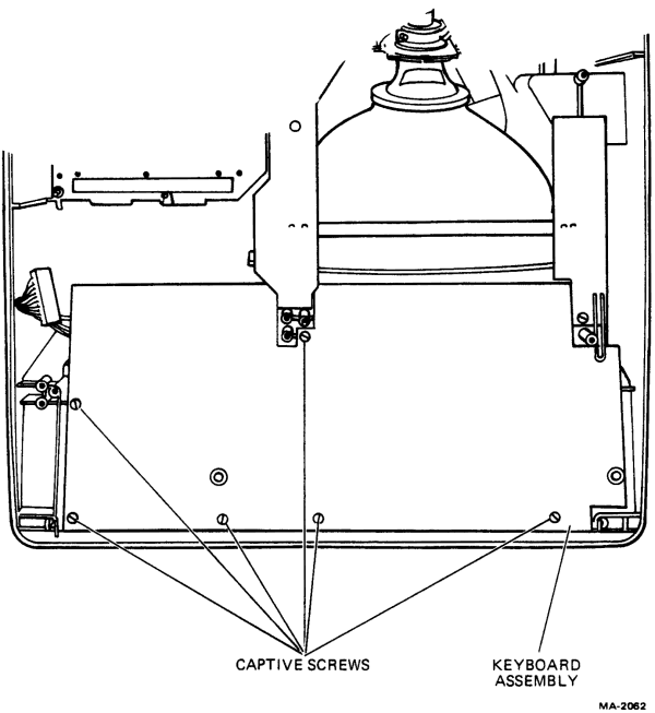
Remove the six hold-down screws from the keyboard module (Figure 5-17).
Lift the keyboard from the terminal.
Figure 5-17 Keyboard Assembly Removal and Replacement
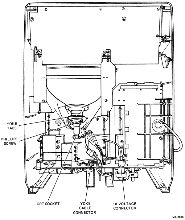
5.3.5 Replacing the CRT Assembly
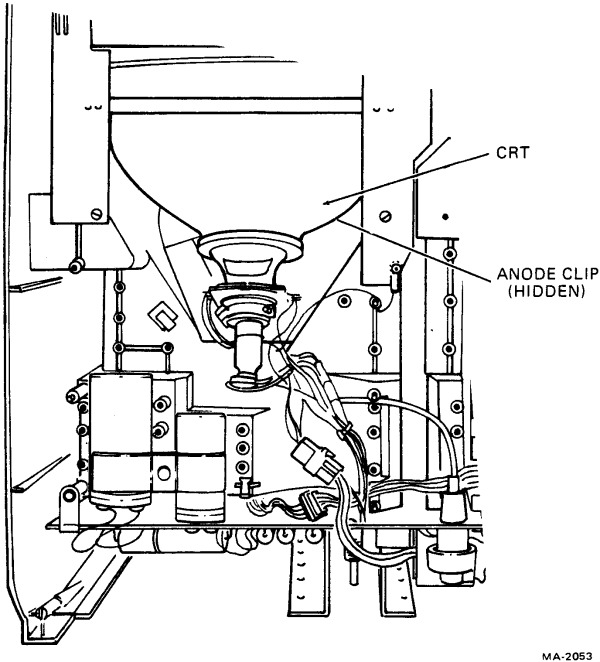
WARNING
There are high voltages present in the power supply
and near the CRT. Make sure the terminal power
line is unplugged and the CRT and capacitors shown
in Figure 5-18 are discharged before handling the
high voltage anode clip and the CRT. Use care when
handling the CRT. The CRT is an evacuated device
and could shatter if broken.
Remove one ground screw if it has the old arcing ECO or unclip one wire if it has the new
ECO.
Remove the screws (as many as ten) holding the new CRT wire form.
Remove two plastic spacers before removing CRT assembly. Be sure to replace the spacers
when CRT is reinstalled.
Lift the CRT assembly out.
Slide a new one in and reassemble the unit.
Figure 5-18 CRT Assembly Removal and Replacement
5.3.6 Replacing the Transformer Assembly
With the unit right-side up, remove the fixed copier cover by first removing the louvered
heat sink plate (four screws) and then pushing the small plastic tab of the cover at the upper
left-hand corner of the shell while lifting on the cover. Notice that the "snap-in" tabs are
molded on and care should be taken when reinstalling the cover that they are securely
fastened. The cover is securely on if, after installing it, you can lift the side of the unit off the
table with your fingers under the serrated edge.
After removing the fixed copier cover, turn the unit on its back and remove the base (Paragraph
5.3.2) and the RUT and the DP modules.
Disconnect the cables leading to the power supply board.
Remove two 8-32 kep-nuts.
Slide out the old transformer assembly and replace it.
Reassemble the unit.
5.4 Display Alignments and Adjustments
Normally, except for the intensity level, no adjustments are required to the terminal after the initial
manufacturing checkout and alignment of the unit. However, after replacing a CRT or deflection
yoke, the display must be realigned and adjusted.
5.4.1 CRT Yoke Alignment
To align the CRT yoke, perform the following:
Remove both covers on the top of the terminal.
Loosen the Phillips head screw securing the yoke to the neck of the CRT (Figure 5-18). If the
screw is inserted so that the head is not accessible (upside down), remove the RUT and DP
modules as directed in Paragraph 5.3.2. Remove the Phillips head screw and insert it in the
opposite direction so that the screw head will be accessible when the terminal is assembled.
Reassemble the terminal but leave the top covers off.
Set up the terminal for local operation as described in Chapter 3 and type a screen full of
characters.
Rotate the yoke until the display is straight. Do not center the display at this time.
Tighten the Phillips head screw until the yoke is snug.
Adjust the yoke tabs as necessary to center the display (Figure 5-18).
Replace the top covers.
5.4.2 Display Adjustments
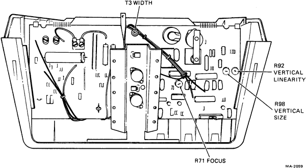
All adjustments are located on the monitor/power supply board. Remove the rear louver plate assembly
as described in Paragraph 5.3.3. Set the unit to the off-line mode of operation as described in
Chapter 3 and fill the screen with characters before making any adjustments. Refer to Figure 5-19 for
locations of the adjusting coil and potentiometers.
Figure 5-19 Alignment Control Adjustment Locations
5.4.2.1 Height
Adjust the vertical-size potentiometer (R98) until the height of the display is 114 mm or 4.5 inches.
This measurement is from the upper edge of the top character line to the lower edge of the bottom
character line.
5.4.2.2 Width
Using a non-conductive hexagonal-tipped alignment tool, adjust the iron slug in coil T3 until the width
of the display measures 218 mm or 8.6 inches.
5.4.2.3 Vertical Linearity
Adjust the vertical linearity potentiometer (R92) until the characters displayed on the top line are the
same size as the characters displayed on the bottom line.
5.4.2.4 Focus
Adjust the focus potentiometer (R71) until characters in all sections of the screen are sharp and clear.
5.5 Voltage Checks
If further testing is required to locate the problem, the unit must be tipped back and the base removed.
To scope the monitor waveforms, the unit must be placed upside down with the heat spreader
removed. The base removal procedures are described in Paragraph 5.3. With the unit tipped back and
the base removed, the Monitor/Power Supply connectors J1 and J2 are accessible for measuring the
voltages listed in Table 5-3.
CAUTION
Use extreme care when measuring voltages on J2 of
the Monitor/Power Supply module. The CRT anode
connector carrying 11,000 V is mounted close to this
connector.
If any voltages are incorrect, remove the heat spreader and proceed to Paragraphs 5.5.1,
5.5.2, 5.5.3, or
5.5.4. If the voltages are correct, check the voltages after distribution to other modules.
Table 5-3 Monitor/Power Supply Voltages
Connector/Pin
Voltage
J1-1
+5
J1-2, 4, 6
GND
J1-10
+15
J2-2
-12
J2-3
-5
J2-4
+5 Sense
J2-5
+5
J2-6
+5
J2-7
GND Remote Sense
J2-8, 9, 10
GND
Table 5-4 Distributed Voltages
Connector/Pin
Voltage
RUT/DP J1-16
GND
RUT/DP J1-17
+15
RUT/DP J1-18
-12
RUT/DP J1-19
+5
RUT/DP J2-1
+5
RUT/DP J1-8
+5
RUT/DP J1-9, 10
GND
RUT/DP J1-45
GND
RUT/DP J1-46
+5
RUT J4-1
+5
RUT J4-2
-12
RUT J4-3
+15
RUT J4-4
GND
RUT/DP J5-9
GND
RUT/DP J11
+5
DP J3-6
GND
DP J3-7
+5
DP J5-8
+15
DP J5-9
-5
DP J5-10
-12
DP J5-11
GND
DP J6-11
+5
5.5.1 Testing the NO VOLTAGE Condition
ACTION:
Ground the collector of transistor Q2 and measure the +15 V supply.
If the voltage measures LOW or 0:
Check for open R1, Q11 or R6; check for shorted Q1; check for short from collector of Q11 to ground.
If the voltage measures +15 or HIGH:
Check for open Q2, D6, D5 or R27; also check R10, R28.
5.5.2 Testing the +15 V Supply
CONDITION:
+5 measures 0 V
ACTION:
Connect the base of transistor Q9 to the collector of transistor Q6.
If the voltage measures LOW or 0:
Check for open Q8, Q9, or R35; check for a short to ground at
the collector of Q8.
If the voltage measures +5 or HIGH:
Check for open Q6, R42, R41; Check for shorted Q5 or faulty E3.
CONDITION:
+5 measures HIGH.
ACTION:
Short the base to the emitter of Q9.
If the voltage measures LOW or 0:
Measure pin 6 of E3. If pin 6 = 0, Q6 is shorted. If pin 6 = 8 V,
check for open R33 or R36; also check R40 and E3.
If the voltage measures +5 or HIGH:
Check for shorted Q8 or Q9.
CONDITION:
+5 measures LOW.
ACTION:
Short the collector to the emitter of Q6.
If the voltage measures LOW or 0:
Check for open Q8, Q9; check R34.
If the voltage measures +5 or HIGH:
Check for open Q6, R40; check for faulty E3, Q5, R35, D12,
R37, R38, R41.
5.5.4 Testing the -12 V Supply
CONDITION:
-12 measures 0V.
ACTION:
Short the collector of transistor Q4 to ground.
If the voltage measures LOW or 0:
Check for shorted Q3; check for open R52, Q12, R19, R20;
check for short between ground and the collector of Q12.
If the voltage measures -12 or HIGH:
Check for open Q4, D20; check for shorted D10.
CONDITION:
-12 measures HIGH.
ACTION:
Short the base to the emitter of Q4.
If the voltage measures 0:
Check for faulty E2, R15, R17, R14.
If the voltage measures HIGH:
Check for shorted Q4, Q12.
CONDITION:
-12 measures LOW.
ACTION:
Short the collector of transistor Q4 to ground and measure the voltage.
If the voltage measures low:
Check R19, R21, D20, R25, R52, R22, Q3.
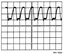
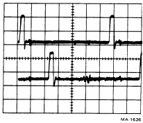
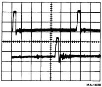
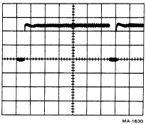
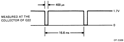
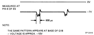
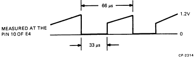
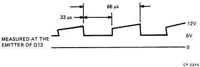
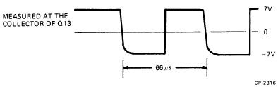
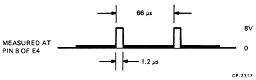
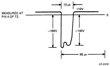
5.6 Timing Waveforms
Figures 5-20 through 5-28 are waveforms of the VT52 timing signals. Included in each figure are the
signal location and the oscilloscope setting for observing the waveform. The serviceman should not
assume that because a signal is present at the indicated pin location it is not suspect. It may be missing
at some other point in the logic due to a broken etch or connection.
For instance, B OSC A, the basic timing clock, may be observed at J1-22 as indicated in the figure but
may be missing at the input to the VSR.
Figure 5-20 B OSC A
Figure 5-21 B OSC A and Shift Register Output
Figure 5-22 Time States TE and TF
Figure 5-23 Time States TE and TW
Figure 5-24 Time States TE and TG
Figure 5-25 Time States TE and TH
Figure 5-26 Time States TE and TJ
Figure 5-27 Sync L
Figure 5-28 Vert H
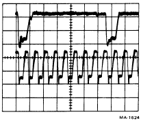
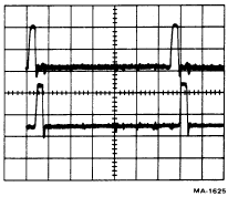
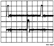
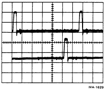
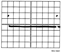
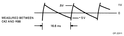
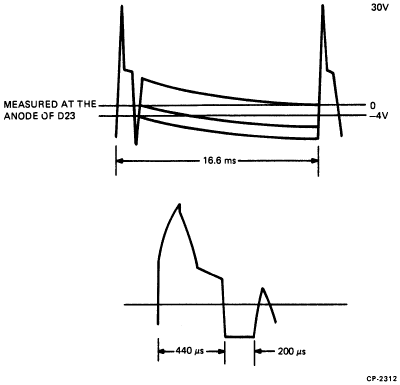
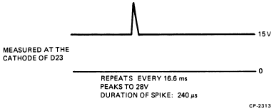
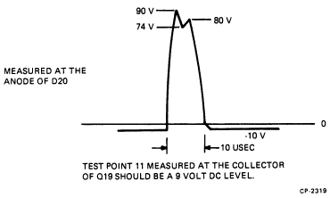
5.7 Monitor Waveforms
The signals illustrated in Figures 5-29 through 5-39 show the normal Monitor waveforms; the waveforms
one would observe in a working VT52 terminal. If the serviceman suspects that the Monitor/Power
Supply module is the cause of some failing condition, he can confirm or reject his
suspicions by comparing the waveforms on the failing unit with the waveforms illustrated in the figures.
Although component level troubleshooting is not recommended when servicing most of the circuitry in
the VT52, the Monitor/Power Supply module can in many cases be serviced to this level because it is
not completely dependent on the microprocessor.