This chapter provides a description of the major functions performed by the VT52. It includes descriptions of the three circuit boards that make up the terminal control logic, the major logic assemblies located on each board, and a functional description of the terminal control features.
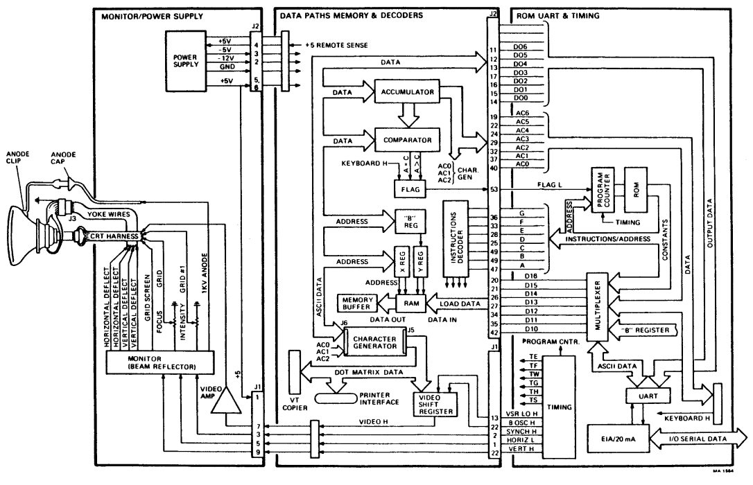
A functional block diagram of the VT52 terminal is shown in Figure 4-1 and should aid the reader in understanding the descriptions presented here.

Three major functions are performed by the VT52 keyboard display. It operates as an input terminal, an output terminal, and a video terminal. As an input terminal, it processes keyboard data and transmits this data to the host processor. As an output terminal, displayable characters received from the host processor are stored in memory and displayed on the screen. As a video terminal, the VT52 displays the contents of main memory on the CRT screen and refreshes this display at the line frequency rate. Main memory consists of 1920 RAM (random access memory) locations used to store the codes for the 1920 characters displayed on the screen (24 rows of 80 characters each). The remaining 128 RAM locations are used as a scratchpad by the microprogram.
In addition to displayable characters, control characters are received at the terminal and are interpreted as commands. Commands exist to position the cursor, erase part or all of the information on the screen, place the terminal in another mode, and force the terminal to identify itself to the host.
The function of the video terminal logic is to fetch ASCII characters from the RAM, convert the ASCII code to one that will form characters in a 7 × 7 dot matrix, and then display these characters on the screen. In order to do this, the video circuits must provide a raster to the screen. That is, reflect the electron beam of the CRT such that, from top to bottom 240* lines are drawn across the face of the screen, 10 lines for each character row. This process is repeated continuously at the line frequency rate: 60 times each second on 60 Hz units; 50 times each second on 50 Hz units. Synchronization of this process is controlled by a crystal oscillator and associated timing circuits. A signal on the cathode of the CRT switches the beam on and off, providing either light (display) or dark (no display).
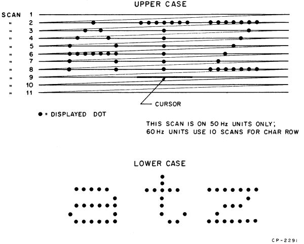
The signal on the cathode is the output of the Video Shift Register which was loaded from the Character Generator. The Character Generator converts the ASCII code received from memory into a code that will form a character on the screen by displaying selected dots of a 7 × 7-dot matrix (Figure 4-2). Character Generator outputs shifted to the CRT cathode represent one line of a 7-line character. Therefore, it takes seven horizontal scans to form a complete character on the screen. In fact, these 7 scans will form 80 complete characters on the screen because during each scan, one line of every character in the row, is displayed.
* On 50 Hz units, the raster consists of 264 lines, 11 lines for each character row.
During each display cycle, 1920 characters stored in the RAM are displayed in the 1920 character positions of the CRT. Character locations in the RAM are identical to character positions on the screen. That is, the code for the character displayed in screen location 0,0 (top, left) will be found in RAM location 0,0 (Y register=0; X register=0). All other characters, 1 through 79, displayed on the top line of the screen will have the same Y address (Y=0) but will have an X address between 1 and 79, i.e., X=1 selects character position 1; X=2 selects character position 2, etc.
At the beginning of every display cycle, when the CRT beam is at the top of the screen, the Y register, X register, and the three least-significant bits of the AC register are cleared to zero. Y=0 and X=0 selects the RAM location containing the character that will be displayed in row 0, column 0 of the screen. AC0,1,2=0 selects the top line of that character. (If one or more scroll operations have been performed, the top character row (row 0) will not be selected when Y=0. This description assumes that no scroll operations have been performed. Scrolling is described in Paragraph 4.5.2).
At T2 time of every timing cycle, the RAM location selected by the contents of the X and Y registers is loaded into the Memory Buffer. The Character Generator is wired to the Memory Buffer. ASCII characters applied to the input of the Character Generator appear at the output in a code that will cause one line of the character to be painted on the screen, when this code is applied to the cathode of the CRT.
The T2 pulse also loads the Character Generator output into the Video Shift Register and increments the X register. In this way, one complete row of characters is automatically fetched from the RAM and displayed during each scan of the video screen. Remember that only one line of each of the 80 characters is displayed during each scan. The displayed line is selected by the decoded output of the three least-significant bits of the AC register. At the beginning of each character row, AC0, 1, and 2 are cleared to zero. At the end of each scan, the AC register is incremented by 1, causing the next line of the same 80 characters to be displayed. After 7 scans, 7 lines of all 80 characters will have been displayed in the character row selected by the contents of the Y register.
There are 10 scans per character row in the 60 Hz terminals; 50 Hz terminals have 11 scans per character row. Seven scans are used to display the characters and the extra scans are used to display the cursor and to provide spacing between the character rows. The cursor is displayed on the scan directly below the last character scan of one of the 24 character rows. The cursor address is stored in scratchpad memory location CUR X and CUR Y. The character format is illustrated in Figure 4-2.
After the last scan, the Y register is incremented by 1 to select the RAM characters to be displayed in the next row, and AC0, 1, 2, and the X register are cleared to zero to select the top line of the character to be displayed in column 0 of the new row. This process continues until 80 characters have been displayed in all 24 rows and is repeated at the line frequency rate. Figure 4-3 is a flow diagram showing the display process.
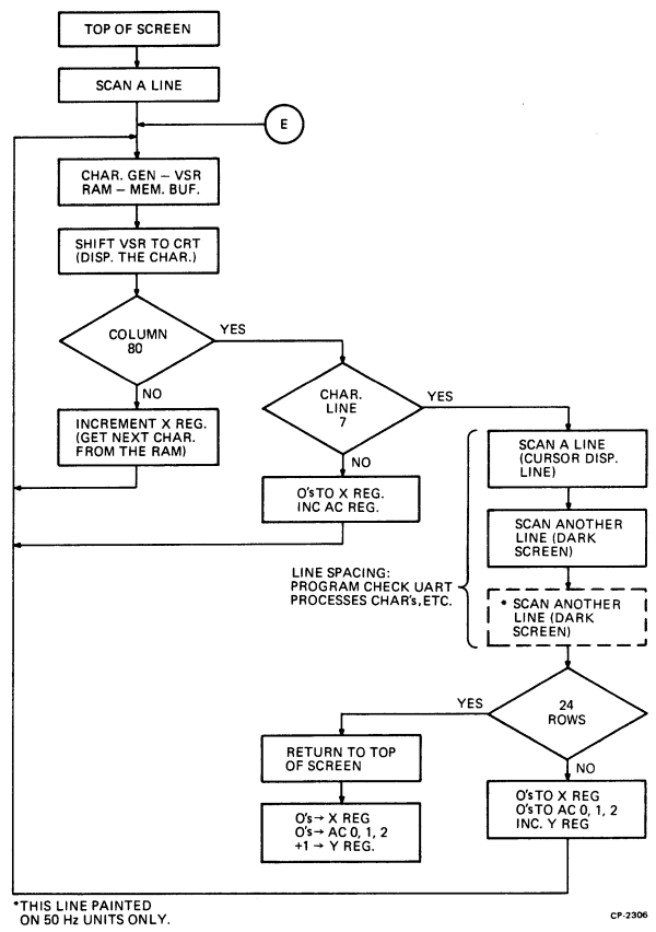
Figure 4-4 is a simplified flow diagram of a keyboard character transmission. Keyboard data entered by an operator is transferred to the host processor under control of the microprogram. Sixty times each second (50 times each second on 50 Hz units), during vertical retrace time, the microprogram checks the keyboard, searching for a typed key. To do this, the program tests the condition of every key in the keyboard. The AC register is set to equal the highest numbered key on the keyboard and then a KEYJ command tests the flag to see if the key is down. If the key is not down, the AC register is decremented and the flag is tested again. This loop is repeated until a typed key is found. When an active key is located, the program stores the identification number of the key in the scratchpad memory to prevent multiple transmission of the same character. The program then looks up the ASCII code for the typed key in a table in the ROM, loads the ASCII character into the UART, and transmits the character to the host.
At the beginning of every keyboard entry routine, the program checks the status of the UART (Universal Asynchronous Receiver/Transmitter). If the UART is still busy transmitting the previous entry, the program makes no further test of the keyboard. If the UART is not busy, the program then tests the keyboard to determine if the previously processed keys are still down. If they are, the program does not process them again. Instead, it exits the keyboard routine. When the previously processed keys have been released, the program resumes keyboard testing.
If none of the keys are down, the program will exit the routine when the AC register is equal to zero. A jumper in the keyboard is wired to act like a typed key whenever it is referenced. It is referenced when the AC = 0, meaning the keyboard was polled but no keys were down.
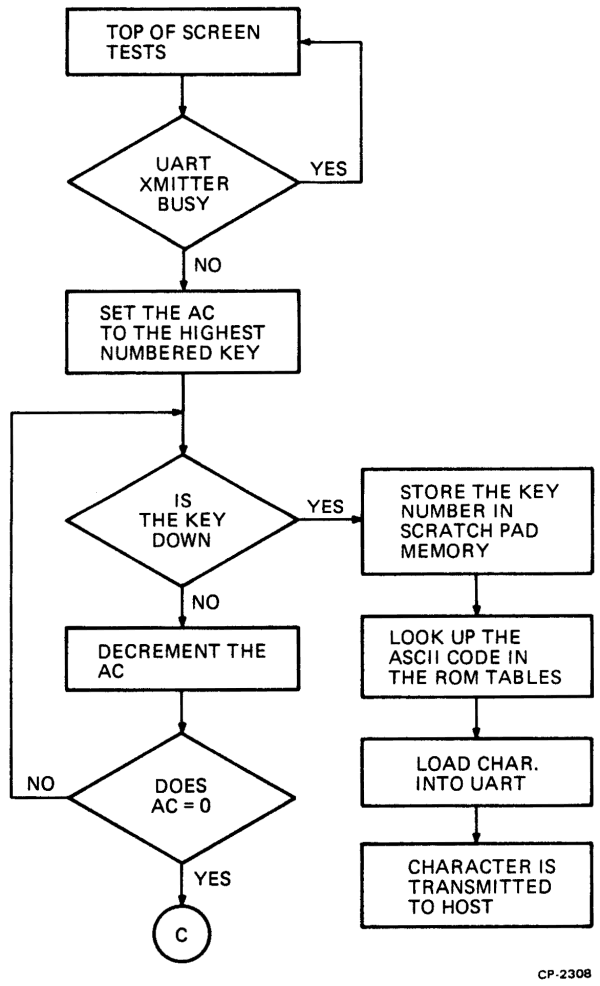
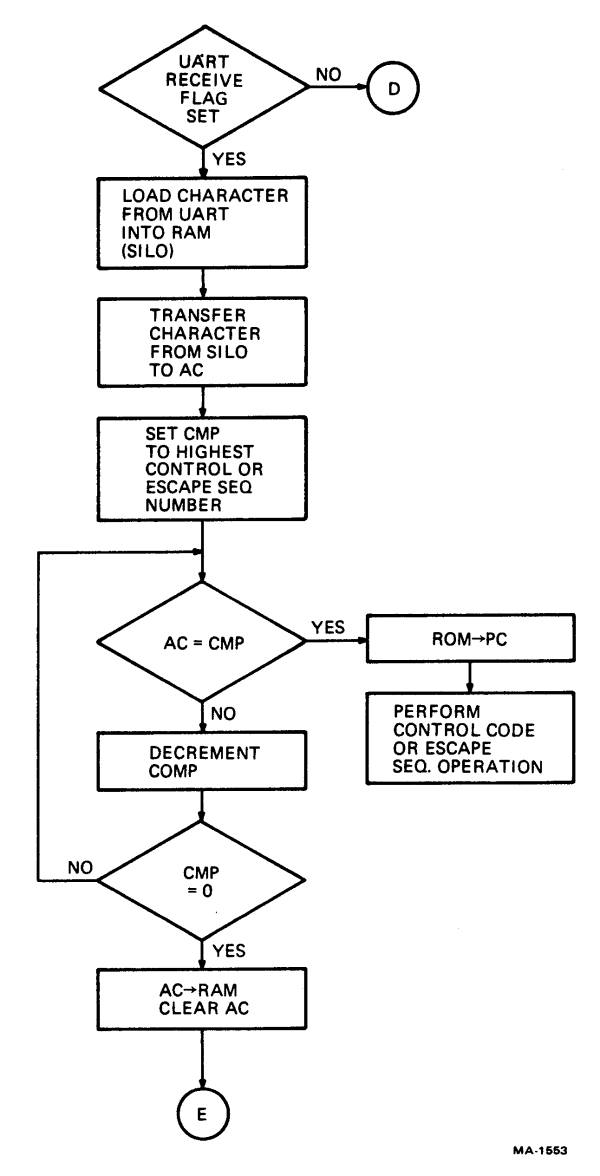
Figure 4-5 is a simplified flow diagram of a received character subroutine. When the UART receiver recognizes a start bit at the data input line, serial data from the host is shifted into the UART by the receive clock. When all bits of the character are in the input buffer, the UART control circuit will set the receive flag UR, TRUE, requesting service from the program. After displaying each character row (during the spacing scans), the program checks the condition of the receiver flag. If UR is TRUE, the program loads the UART character into the RAM location specified by the cursor address (CUR X and CUR Y locations in the scratchpad). The UR flag is then cleared and the cursor address is incremented in preparation for the next character that will be received from the host. Control codes received by the terminal will not be stored in memory or displayed on the screen. They will be interpreted by the terminal as commands and the action defined by that command will be performed, e.g., move the cursor.
The complete logic package for the VT52 has been assembled on three modules: the Data Paths, Memory, and Decoders module (DP); the ROM, UART, and Timing module (RUT); and the Monitor/Power Supply module. The following paragraphs provide a detailed description of the major logic assemblies located on each module.
The RAM and Memory Buffer, the Character Generator, the Video Shift Register (VSR), the instruction decoders, and the Memory Select and Program Test Registers are located on the Data Paths, Memory, and Decoders module. Each of these logic groups will be discussed separately.
4.3.1.1 RAM and Memory Buffer – The RAM consists of fourteen 2102 chips arranged to provide two, 1024 × 7-bit read/write memories (Figure 4-6). To the programmer, the memory appears as a 2048 × 7-bit memory because the RAM addressing scheme assigns all even addresses to one 1024 memory (page 1) and all odd addresses to the other memory (page 2); 1920 locations are used to store a screenful of characters (24 lines × 80 columns); the remaining 128 locations are used by the microprogram as a scratchpad memory, i.e., temporary storage of keyboard characters, cursor address, etc.
The Memory Buffer contains the contents of the RAM location selected by the current contents of the X and Y registers. Twice during each instruction time the selected RAM output is strobed into the Memory Buffer for transfer to the video circuits during display time, or to the UART for transmission to the host processor, or to the X, Y, AC, or B registers because of a command test condition. Data written into the RAM can be from the AC register, the B register, the ROM (Read Only Memory – contains the microprogram), or the UART. These inputs are multiplexed into the RAM by the signals MUX A and MUX B. The TRUE/FALSE condition of MUX A and MUX B is the result of decoded microprogram transfer commands.
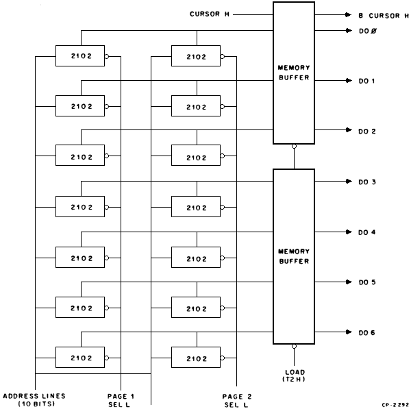
RAM Addressing – As previously stated, the RAM consists of two 1024 × 7-bit memories labeled page 1 and page 2. Page 1 contains all the even locations addressed by the X and Y registers; page 2 contains all the odd locations. Page selection is controlled by the least significant bit of the Y register (not Y0). The X register and Y3, Y2, Y1, and Y0 are decoded to select one of 1024 memory locations; the least significant bit of the 5-bit Y register selects the page. For this discussion then, we will only consider the selection of locations within one of the pages since memory selection in both pages is identical.
Since the RAM contains all the characters displayed on the screen, it is convenient to have the RAM locations reflect the character positions on the screen, i.e., consider the RAM configuration to be 12 × 80*. The 1024-bit RAM cannot be directly addressed to provide this configuration. It requires 10 bits of address information to select one of 1024 locations in memory. If 7 bits are used for column selection, only 3 bits remain to select one of the 12 rows. If 4 bits are used for row selection, the remaining 6 bits are inadequate for selecting one of 80 columns. To solve the program, address mapping is used (Figure 4-7). That is, by manipulating some of the address lines, the operator/programmer is allowed to think of the RAM as a 12 × 80 configuration.
* Although the VT52 displays 24 rows, Y register decoding selects only 12, page-selection provides the other 12.
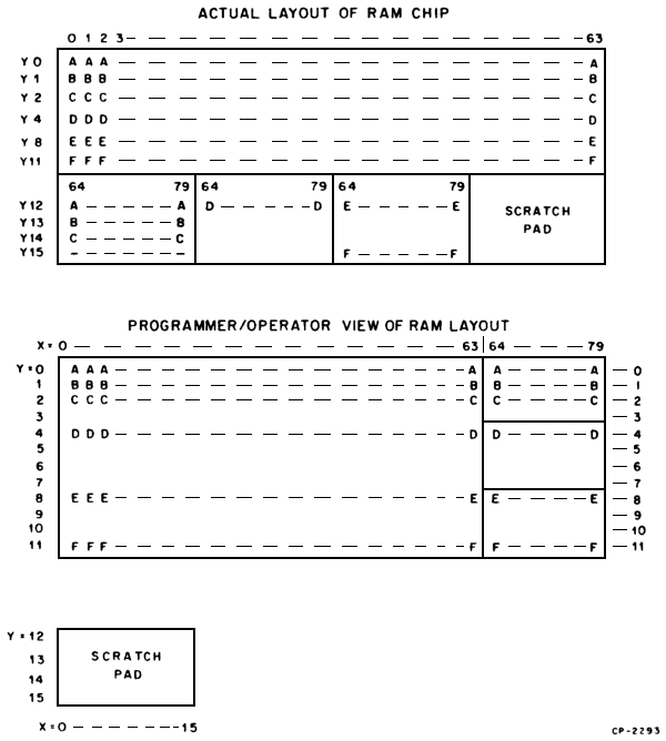
Figure 4-7 illustrates how the address mapping is accomplished. The memory is arranged in a 16 × 64 configuration with Y3, Y2, Y1, and Y0 selecting one of 16 rows and X5, X4, X3, X2, X1, and X0 selecting one of 64 columns. Whenever the X register <= 64, or the Y register <= 12, the two most significant Y address lines are forced high and the two most significant X address lines are replaced by Y3 and Y2. This effectively divides the RAM into five sections: one 12 × 64 section and four 4 × 16 sections. Memory references for characters displayed in columns 0 through 63 will be made to the 12 × 64 section; memory references for characters displayed in columns 64 through 79 will be made to one of three 4 × 16 sections. The contents of the Y register will determine which one of the three 4 × 16 sections will be referenced.
The remaining 4 × 16 section is used as a scratchpad memory by the microprogram. This section is addressed whenever the Y register contains a number greater than 11. The address mapping circuits replace the two most significant bits of the X register selection bits with Y3 and Y2. Since Y3 and Y2 will both contain 1s when a number greater than 11 is in the Y register, they will select the highest 4 × 16 memory section. X3, X2, X1, and X0 will select one of the 16 locations in this section. Uses of the scratchpad are described in the microprogram section.
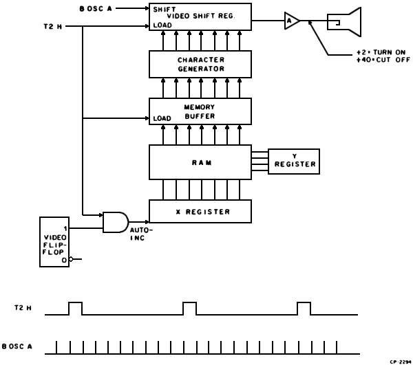
4.3.1.2 Video Shift Register (VSR) – The VSR is a 7-bit shift register that holds one line of the 7-line character currently being displayed on the CRT screen. During each video scan, the VSR is loaded from the Character Generator 80 times, once for each character position. After loading, the contents of the VSR are shifted by B OSC A, the basic timing clock, through the video amplifier to the cathode of the CRT where they modulate the electron beam. Signal 0s shifted out of the VSR will cause a +2 V signal on the cathode, and light on the screen. Signal 1s will cause a +40 V signal on the cathode cutting off the CRT and producing a dark screen.
Figure 4-8 illustrates the data path of the character from the RAM to the CRT cathode. Display timing is also illustrated in the figure. T2H, a timing pulse that occurs once every timing cycle, simultaneously loads the VSR with one line of the character to be displayed and loads the Memory Buffer with the character that will be displayed in the following screen location. Assume the terminal is ready to display a line starting in column 0, and assume the display characters to be an A in column 0, a B in column 1, a C in column 2, etc. At T2H time, one line of the display code for A is loaded into the VSR and the ASCII code for B is loaded into the Memory Buffer. The X register is incremented, selecting the RAM location containing the ASCII code for C. While B OSC A shifts A to the CRT, the Character Generator is encoding the B into a display code, and the ASCII code for C is settling at the input to the Memory Buffer.
4.3.1.3 Decoders – Every operation performed by the VT52 is the result of an instruction stored in the 1024 × 8-bit ROM. The 8-bit ROM word is decoded by the decoder logic to produce an instruction. This instruction will cause some action to take place in the terminal. The bits of the ROM word are labeled A, B, C, D, E, F, G, H.
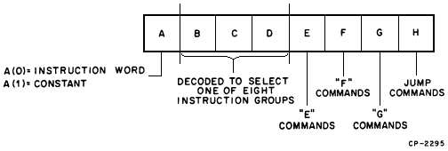
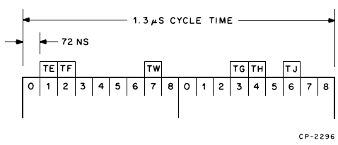
As Figure 4-9 shows, the ROM word is divided into three groups: A, BCD, and EFGH. If bit A = 0, bits B, C, and D are decoded into one of eight instruction groups. Bits E, F, G, and H are sampled to determine what action is to be taken. An action occurs if one of more of the bits are set to 1. For example, if bit E is a 1, a certain action will occur; if bits E and F are both set to 1, two actions will occur but not at the same time. If E, F, G, and H are all set to 0, a different action takes place depending on the state of B, C, and D. Table 4-1 is a list of VT52 commands that are available when ROM bit A is set to 0. If bit A of the ROM word is set to 1, a load RAM from ROM command will be decoded. When operating in mode 1, the command is unconditional. The seven least significant bits of the ROM word, BCDEFGH, are loaded into the RAM location specified by the contents of the X and Y registers. When operating in mode 0, the load command is conditional. In operation, the command increments the AC register and then compares the AC to the selected RAM location. If AC < RAM, the load command is not performed, i.e., the contents of the selected RAM location remain unchanged. If AC > RAM, BCDEFGH are loaded into the RAM and the DONE flip-flop is set. All instructions listed in Table 4-1 are decoded at specific times in the instruction cycle. Six time states are produced during each instruction cycle (Figure 4-10) TE, TF, TW, TG, TH, and TJ. These signals are gated with ROM bits EFGH to enable the desired action. Table 4-2 lists the timing states and the instructions performed at each state in the instruction cycle.
| ABCD | E | F | G | H | Instruction | Mnemonic |
|---|---|---|---|---|---|---|
| 0000 | 0 | 0 | 0 | 0 | Set Cursor flip-flop | (SCFF) |
| 1 | X | X | X | Clear the X and Y registers | (ZXZY) | |
| X | 1 | X | X | Decrement the X and Y registers | (DXDY) | |
| X | X | 1 | X | Load AC from memory | (M2A) | |
| X | X | X | 1 | Mode 0: Printer scan flag set? | (PSCJ) | |
| Mode 1: Jump if UART has received a character | (URJ) | |||||
| 0001 | 0 | 0 | 0 | 0 | Set Video flip-flop | (SV1D) |
| 1 | X | X | X | Complement bit X3 (8s-bit) of X register | (X8) | |
| X | 1 | X | X | Increment AC register | (IA) | |
| X | X | 1 | X | Load RAM from AC | (A2M) | |
| X | X | X | 1 | Mode 0: Jump if AC0, 1, 2 = 78 | (TABJ) | |
| Mode 1: Jump if AC = RAM | (AEMJ) | |||||
| 0010 | 0 | 0 | 0 | 0 | Load Y register from Y buffer | (B2Y) |
| 1 | X | X | X | Increment X; decrement Y | (IXDY) | |
| X | 1 | X | X | Increment AC register | (IA1) | |
| X | X | 1 | X | Load UART from RAM | (M2U) | |
| X | X | X | 1 | Mode 0: Jump if key-click | (KCLJ) | |
| Mode 1: Jump if AC < RAM | (ALMJ) | |||||
| 0011 | 0 | 0 | 0 | 0 | Complement Bell flip-flop | (CBFF) |
| 1 | X | X | X | Increment X register | (IX) | |
| X | 1 | X | X | Increment Y register | (IY) | |
| X | X | 1 | X | Load RAM from B register | (B2M) | |
| X | X | X | 1 | Mode 0: Jump if 60 Hz line frequency | (FRQJ) | |
| Mode 1: Jump if AC /= X register | (ADXJ) | |||||
| 0100 | 0 | 0 | 0 | 0 | Clear cursor and Video flip-flop | (ZCAV) |
| 1 | X | X | X | Clear AC register | (ZA) | |
| X | 1 | X | X | Decrement Y register | (DY) | |
| X | X | 1 | X | Load X register from RAM | (M2X) | |
| X | X | X | 1 | Mode 0: Printer request flag set? | (PRQJ) | |
| Mode 1: Jump if AC = RAM | (AEM2J) | |||||
| 0101 | 0 | 0 | 0 | 0 | Load Print Shift register | (LPB) |
| 1 | X | X | X | Enter Mode 1 | (M1) | |
| X | 1 | X | X | Increment ROM Bank | (IROM) | |
| X | X | 1 | X | Load RAM from UART | (U2M) | |
| X | X | X | 1 | Mode 0: | (TRUJ) | |
| Mode 1: | ||||||
| 0110 | 0 | 0 | 0 | 0 | Start printer | (EPR) |
| 1 | X | X | X | Clear X register | (ZX) | |
| X | 1 | X | X | Decrement X register | (DX) | |
| X | X | 1 | X | Load Y buffer from RAM | (M2B) | |
| X | X | X | 1 | Mode 0: Jump if UART is transmitting | (UTJ) | |
| Mode 1: Jump if video flag scan | (VSCJ) | |||||
| 0111 | 0 | 0 | 0 | 0 | Halt printer and clear Y register | (HPR!ZY) |
| 1 | X | X | X | Enter Mode 0 | (M0) | |
| X | 1 | X | X | Decrement AC register | (DA) | |
| X | X | 1 | X | Spare | ||
| X | X | X | 1 | Mode 0: Jump if not top of screen | (TOSJ) | |
| Mode 1: Jump if key not typed | (KEYJ) | |||||
| Time State | Decoded Instruction | ROM Enabling Signals |
|---|---|---|
| TE | ZXZY, X8, IXDY, IX, ZA, M1, 2X, M0 | A · E |
| TF | DXDY, IA, IA1, IY, DY, IROM, DX, DA | A · F |
| TW | SCFF, SVID, B2Y, CBFF, ZCAV, LPB, EPR, HPR!ZY | A · E · F · G · H |
| TG | CLEAR the WRITE FLIP-FLOP | |
| TH | M2A, A2M, M2U, B2M, M2X, U2M, M2B | A · G |
| TJ | JUMP, NO-OP | A · H |
4.3.1.4 Character Generator – The Character Generator consists of a 1024 × 8-bit ROM and associated address gating. The display code for all characters displayed on the screen is stored in the ROM.
During display scans, characters fetched from the RAM are loaded into the Memory Buffer in ASCII format. Because the address selection lines of the Character Generator are wired directly to the Memory Buffer, the Character Generator never needs to be "loaded"; it is always selecting the ROM location addressed by the ASCII code in the Memory Buffer. For example, if the Memory Buffer contains the ASCII code for A (1018), the Character Generator address lines will select the ROM location containing the 7 × 7 display code for the letter A. However, since the character display method used by the VT52 requires that only one line of the 7 × 7 character be displayed during a single horizontal scan, three more address lines are provided to select one of the seven lines of the matrix; the three least-significant bits of the AC register. In operation, ASCII characters are loaded into the Memory Buffer; the Character Generator uses this code as an address to select the ROM location containing the display code for the desired character. AC bits 0, 1, and 2 are decoded to select one of the seven lines of the character matrix for output to the Video Shift Register.
Character Generator outputs CD0-6 are loaded into the Video Shift Register during T2 time of every clock cycle. CD6 will be the first bit shifted out of the VSR; CD0 will be the last.
The ROM with resident microprogram, the Program Counter (PC), the basic clock and timing chain, and the Universal Asynchronous Receiver Transmitter (UART) are located on the RUT module.
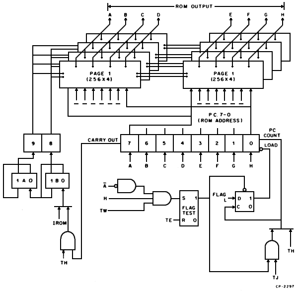
4.3.2.1 ROM and PC – The ROM is a 1024 × 8-bit read-only memory that stores the VT52 microprogram. It consists of eight 256 × 4-bit chips organized as illustrated in Figure 4-11 to provide four pages of 256 × 8-bit memory. The outputs ABCDEFGH reflect the contents of the location addressed by the Program Counter (PC). The eight least significant bits of the PC will address one 8-bit ROM word from page 1, 2, 3, 4. Page selection is determined by the condition of PC bits 8 and 9. The PC is normally counted at TH time of every instruction cycle to fetch a new command or address from the next sequential ROM address.
Commands that affect the PC and the ROM are JUMP and IROM. A program jump is accomplished by loading a new address into the PC. The new address is always the contents of location JUMP + 1. At TH time of the JUMP command, the PC is counted and the ROM output word will contain the new address (JUMP + 1). If the jump conditions have been met, FLAG L will be TRUE and PC COUNT will load the new address into the PC. Program skips are the result of not meeting JUMP conditions; there is no skip command. If JUMP conditions are not met, FLAG L will be false and the PC will not receive the new address. Instead, PC COUNT will increment the PC a second time, fetching the next command from location JUMP + 2.
The JUMP command just described allows jumping within the selected page. To jump to a different page, the program must perform one or more IROM commands followed by a jump command. The IROM command increments the page counter (flip-flops A and B in Figure 4-11) and when a jump command is executed, the new page address is loaded into PC9 and PC8. At the same time, the contents of ROM location JUMP + 1 are loaded into PC7 through PC0 to select one of the 256 locations in the new page.
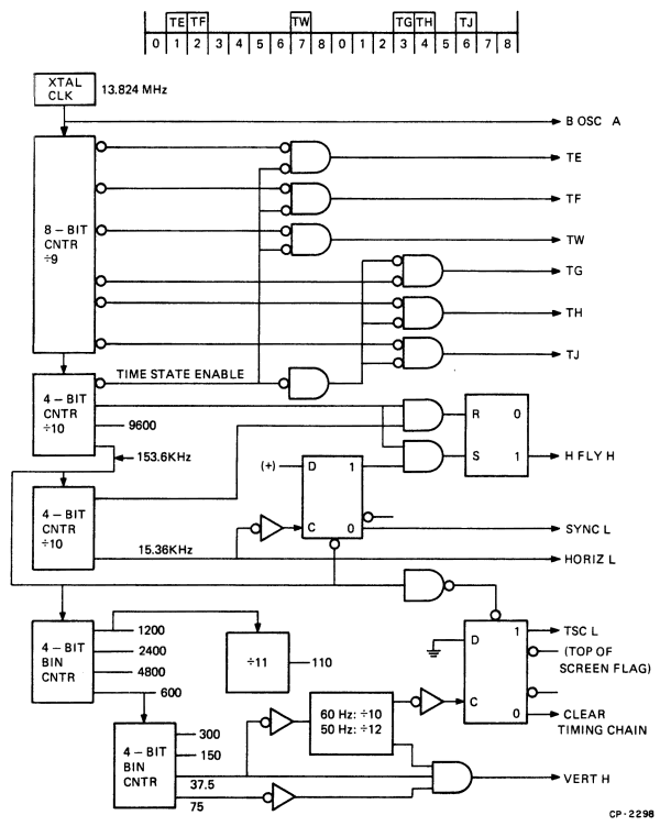
4.3.2.2 Timing – All operations in the VT52 are synchronized by the basic timing clock and timing chain (Figure 4-12). The clock is a crystal-controlled oscillator operating at 13.824 MHz. Clock output B OSC A provides the basic clock frequency for the timing shift register and frequency dividers. It is also used to perform shift operations in the Video Shift Register. The output of the crystal clock becomes the input clock of an 8-bit shift register. The outputs of the shift register are ANDed together to provide an input data signal to the register. When all bits in the register are set to 1, the input data signal will be "0"; at all other times, the input data signal will be a "1". The result is that the register acts like a 9-bit ring counter with a "0" being shifted through all of the bit positions.
The output from this register when ANDed with the TIME STATE ENABLE signal produces the six time state signals required by the VT52 for instruction decoding. The TIME STATE ENABLE signal is the output of the first stage of a 4-bit divide-by-10 counter that follows the shift register in the timing chain. The input clock to this counter is wired to the last stage (bit 7) of the shift register. This means that the TIME STATE ENABLE flip-flop is toggled once for each complete cycle of the shift register. It also means that it takes two complete cycles of the shift register to produce the six time state signals.
The input clock frequency applied to the 4-bit decade counter is 1.536 MHz which is the crystal clock frequency divided by 9. Since this is a divide-by-10 counter, the frequency at the final stage will be one-tenth of the input frequency, or 153.6 kHz. The 9600-baud clock is taken from this counter (baud rate × 16 = clock frequency).
The clock is again divided by 10 in a second decade counter producing an output frequency of 15.36 kHz which is the horizontal display frequency. The output of the final stage of this counter is signal HORIZ L which is at ground level during horizontal retrace time. The high-to-low transition of this signal clocks the SYNC flip-flop enabling SYNC L to the flag multiplexer. The SYNC transition clocks another flip-flop producing H FLY H which inhibits automatic incrementing of the X register and the loading of the VSR.
The clock is fed to three more counters to produce the clocks for the rest of the baud rates available in the VT52. The last counter in the timing chain is used to develop the vertical display synchronization signal, VERT H. This counter is jumper selected to divide by 10 or divide by 12 to produce a 60 Hz or 50 Hz VERT H signal.
4.3.2.3 Interface Module – The interface may be a 20 mA current loop interface or an EIA standard interface; customer specified. Each interface is mounted on a 2 × 6 adapter card and connector J1 on the card connects directly to the ROM, UART, and Timing module connector, J4. Cables are supplied with both interfaces for connecting the terminal to a host processor or a modem. Table 4-3 lists the signals that connect the terminal to the interface.
| Terminal Connection | Interface Connection | Signal |
|---|---|---|
| RUT/J4-1 | J1-1 | +5 |
| RUT/J4-2 | J1-2 | -12 |
| RUT/J4-3 | J1-3 | +15 |
| RUT/J4-4 | J1-4 | Ground |
| RUT/J4-5 | J1-5 | Received Data |
| RUT/J4-7 | J1-7 | Transmitted Data |
20 mA Adapter Card* – The 20 mA adapter card is supplied with a 4-meter, No. 22 AWG stranded 4-wire cable that terminates in an 8-pin Mate-N-Lok connector. Table 4-4 lists the cable signal names.
* Unless otherwise specified, the 20 mA current loop interface is shipped in VT52 terminals.
| Mate-N-Lok Pin No. | Signal Name | Color |
|---|---|---|
| 7 | Transmitted Data (+) | Green |
| 3 | Transmitted Data (-) | Red |
| 5 | Received Data (+) | White |
| 2 | Received Data (-) | Black |
EIA Adapter Card – The EIA adapter card is supplied with a 7620 mm cable terminating in a 25-pin, MALE CANNON DB 19604-432 or equivalent connector. Table 4-5 lists the cable signal names.
| Cannon Pin No. | Signal Name | Comments |
|---|---|---|
| 1 | Protective Ground | Logic 1 = OFF = -10 V |
| 2 | Transmitted Data | Logic 0 = ON = +10 V |
| 3 | Received Data | Logic 1 = OFF = -5 to -25 V Logic 0 = ON = +5 to +25 V |
| 4 | Request to Send | Wired TRUE (+10 V) |
| 7 | Signal Ground | |
| 20 | Data Terminal Ready | Wired TRUE (+10 V) |
| All others | No connection |
4.3.2.4 UART – The UART is a full-duplex receiver/transmitter that accepts asynchronous, serial binary characters from the host processor and converts them to parallel format for transfer to the RAM. It also accepts parallel binary characters from the RAM, converts them to serial data with added START and STOP bits and transmits this data to the host processor. The send/receive frequency of the UART (baud rate) is selected by setting switches S1 and S2 located at the front, bottom of the unit, under the keyboard.
The VT52 will transmit data with odd parity, even parity, or no parity. A parity switch (S3) and two jumper slots located under the keyboard are used for parity selection. Switch positions are NONE and EVEN. If the switch is set to NONE, the UART will transmit mark parity, i.e., the parity bit is always a "1" regardless of the number of 1 bits in the word. If a jumper is inserted in slot W5, a "0" will always be transmitted in the parity bit (space parity). Odd parity can be selected by setting switch S3 to EVEN and adding a jumper in slot W6. The terminal ignores parity on received data.
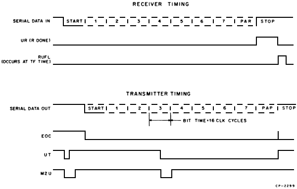
Transmitting – To transmit a character to the host, the microprogram checks UART status signal UT and if the UART is not busy, the program does a Memory-to-UART (M2U) transfer. This transfer loads the contents of the selected RAM location into the input data buffer of the UART. UART control then loads the character into the output shift register allowing the X CLK to transmit the character to the host. While shifting the data, parity is calculated and then appended to the data followed by the stop bit(s). The End-of-Character (EOC) flag is set and remains in this state until a new character is transferred from the input buffer to the output shift register. Status signal UT goes TRUE when a character is transferred from the input buffer to the shift register to alert the microprogram that it is ready for another character. Figure 4-13 shows the UART timing.
Receiving – Serial input data from the host processor is shifted into the receive shift register by the receive clock (R CLK) upon receipt of a START bit on the serial input pin. When the STOP bit is recognized, the character is transferred to the output data buffer and signal UR goes TRUE signaling the program that a character has been received. (The program checks UART status after displaying each character row). A UART-to-Memory (U2M) command transfers the character to the RAM location specified by the cursor if the received code is a displayable character. At TF time of the transfer command, flip-flop RUF will set, producing RUF L which clears the UR signal flag. Refer to Figure 4-13 for UART timing.
The monitor includes a cathode ray tube, horizontal and vertical deflection circuits to position the electron beam leaving the cathode, and a video amplifier to modulate that beam with the signal from the Video Shift Register.
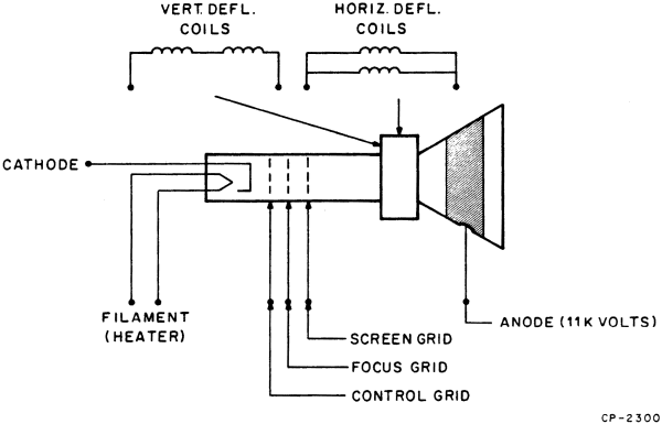
4.3.3.1 The CRT – Figure 4-14 is a diagram of the cathode ray tube used in the VT52. It consists of a heater, an electron-emitting cathode, a control grid for biasing, a focus grid for shaping the beam, a screen grid for accelerating the beam, and a high voltage anode for attracting the beam to the phosphor-coated face of the tube (screen). The beam strikes the screen at a high velocity causing the phosphor to give off light. Magnetic fields, produced by driving current through the horizontal and vertical deflection coils (yoke drivers), deflect the beam left and right, and up and down. The angle of deflection is proportional to the strength of the magnetic field, which is proportional to the current flowing through the coil.
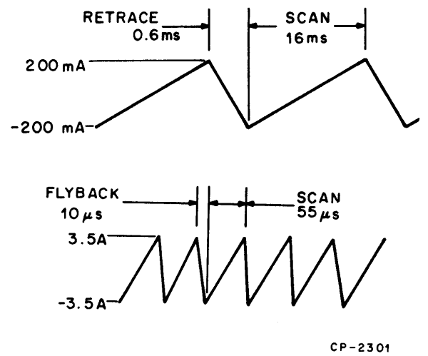
4.3.3.2 Beam Deflection – As stated in Paragraph 4.3.3.1, field strength is proportional to current. Therefore, if the current through the coils is steadily increased, the magnetic field will also increase and the beam will deflect from left to right and from top to bottom, an amount proportional to the increase in current. If the currents are quickly returned to their original value, the beam will quickly return to its original position.
Figure 4-15 shows the horizontal and vertical sawtooth current waveforms through the deflection coils. Vertical deflection is very slow compared to horizontal deflection. This is because 240 horizontal scans occur for each vertical scan in 60 Hz units; 50 Hz units have 264 horizontal scans per frame. During vertical retrace time, the beam makes 16 additional horizontal scans.
Yoke Drivers (Refer to Monitor/PS Drawing D-CS-5410886-0-1, sheet 3) – Due to a large change in voltage per unit time and greater angle of deflection required, most of the voltage drop across the horizontal yoke is through inductance whereas, in the vertical yoke, resistance is more significant than inductance in causing the voltage differential. For this reason the two driver circuits are designed differently.
Vertical Yoke – At the center of the driving circuit for the vertical yoke is an operational amplifier (E5) in a current-sampling integrator configuration (with capacitor C42). The basic functional circuit is shown in Figure 4-16.
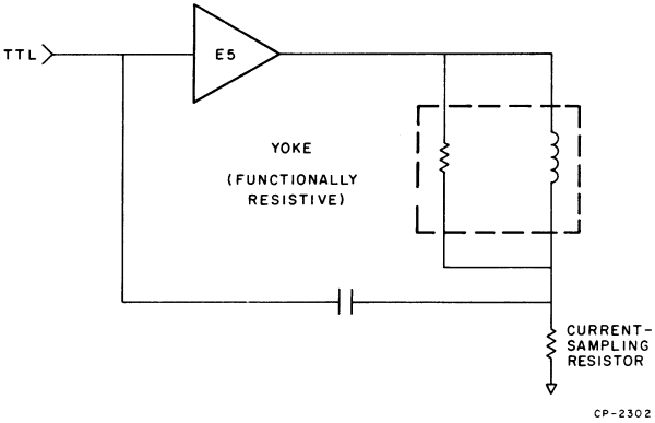
A power-driver stage is added by an emitter-follower (transistors Q16 and Q17). Transistor Q18 serves as a voltage-level converter. It is a common-emitter amplifier. To prevent dc leakage current from flowing through the vertical yoke, a capacitor is put in series with it. In addition, feedback is brought from the yoke back to the operational amplifier. E5’s gain is 1 under dc conditions, when the resistance between the inverting input (pin 2) of E5 and ground is 100 kΩ; under ac conditions, C40 lowers that resistance to 10 kΩ, giving E5 a gain of 10. This ensures saturation of the output of the operational amplifier, which makes the flyback cycle more effective.
Diode D23 charges capacitor C31 during vertical retrace. This reduces the current requirements of the vertical circuit during the downward scan, since it uses the energy stored in the capacitor.
Horizontal Yoke – The horizontal yoke is basically an inductor. By supplying a constant voltage, a constantly rising current will result which causes the horizontal scan. The momentum of this current across the coil is used to charge a capacitor which supplies the reverse voltage needed in flyback. This capacitor and the yoke form a resonant circuit. A diode is added to keep the capacitor from ringing after flyback has been achieved. As a result of flyback, the high current in the reverse direction is also sent to T1, the flyback transformer where it performs several functions:
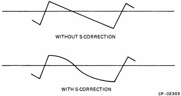
Again, there is a capacitor in series with the yoke. As well as eliminating dc across the yoke, it supplies the S-correction (Figure 4-17) to the yoke. It was mentioned before that the angle through which the yoke deflects the electron beam varies directly with the current through the yoke. But this does not result in a constant rate of speed of the beam’s travel across the screen; since all the points on the screen are not an equal distance from the source of the electron beam, a deflection of 1 degree, when the beam is at the center, would produce less distance change than the same deflection when the beam is at an edge of the screen. The capacitor performs S-correction by slowing down the movement of the electron beam when it is near the edges.
A variable inductor (T3) in series with the yoke is used to provide adjustment of the width of the scan.
The other coil in series with the yoke, T4, is the linearity coil. Its non-linear inductance corrects for some of the second-order effects; the resistance of the yoke and some of the voltage drops in the circuit.
The circuit at coordinates D3 uses the SYNC signal as the time base to integrate voltage sampled from pins 8 and 9 of the flyback transformer T1. A fast power transistor, which has started flyback too early with respect to the SYNC signal, will allow more current to be integrated. This circuit will compensate for the power transistor’s fast storage by increasing its base current, which will slow it down. A power transistor which is too slow will likewise be compensated for by reducing its base current. Another benefit of this circuit is to guarantee that the power transistor will always be saturated when the horizontal scan begins, which will ensure its linearity.
Video Circuits – The screen grid provides +360 V in order to accelerate the electrons emitted from the cathode to the screen.
The focus circuit supplies a voltage from 0 V to 450 V to the focus grid. R71 is used to adjust this voltage to obtain the sharpest picture on the screen.
The intensity circuit supplies from 0 V to -80 V to the control grid. R93, which is the operator control at the rear of the unit, is used to fix this voltage, regulating the general intensity of the screen. A more negative voltage will suppress the flow of electrons to the screen, producing a dimmer image.
The two levels of intensity that are used to display characters on the screen are produced as Q21 switches on and off. This will take the cathode from +40 V (dark) to +2 V (light). D37 prevents Q21 from saturating, ensuring high speed of operation.
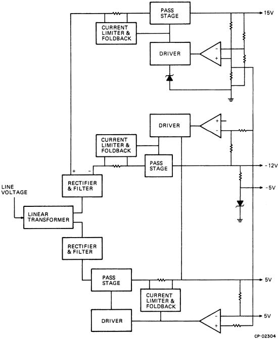
4.3.3.3 Power Supply – The power supply is located on the same module as the monitor electronics. It provides four voltages to the terminal electronics: (+)15 V, (-)12 V, (-)5 V, and (+)5 V. The voltage distribution is as shown in Table 4-6. Figure 4-18 is a block diagram of the power supply.
The linear transformer has a flux shield optimally positioned to prevent interaction between the flux generated by the transformer and the electron beam of the CRT, which should produce, if the line frequency varied from the nominal, a phenomenon known as "swimming". Current goes into a full-wave rectifier with center-tap. The positive and negative outputs of this rectifier are regulated to +15 V and -12 V respectively.
| Voltage | Use |
|---|---|
| +15 | Horizontal and Vertical Deflection Circuits and EIA Interface Option |
| -12 | Vertical Deflection Circuit and EIA Interface Option UART Character Generator |
| -5 | Character Generator Bias |
| +5 | TTL Logic and RAM |
Another winding of the transformer is passed through a full-wave center-tap rectifier and capacitor-input filter to be regulated to +5 V. The power supply of +15 V, -12 V, and +5 V uses only one voltage reference, utilizing a Zener diode. (The -5 V supply uses its own Zener diode).
Each rectifier has current-limiting and foldback to protect against inadvertent short-circuits during maintenance or for any other reason.
The keyboard is arranged so that the keys form an 8 × 10 matrix and every key except the BREAK key has been assigned a unique identifying number representing its position in the matrix. The AC register is used to detect keys that have been activated (typed). AC0, 1, and 2 are decoded to enable one of the eight lines of the matrix; AC3, 4, 5, and 6 are decoded to enable one of the 10 columns. Any key can be checked by placing its identifying number into the AC register. If the key is not down, FLAG L will be TRUE, causing a program JUMP when instruction KEY J is executed.
The program polls the keyboard during vertical retrace time by loading the AC register with the highest key number and entering a program loop that continually subtracts 1 from the AC register and tests the result until an active key is found or until the AC=0.
When a key is found "down", the program leaves the test loop and stores the key number in location Keyboard A or Keyboard B of the scratchpad memory. On subsequent keyboard pollings, the program will fetch the numbers stored in Keyboard A and Keyboard B and check the keyboard to see if one or both of these keys are still "down". If both keys are down, the program leaves the loop and no keyboard entries are made. When either of these keys are found to be "up", scratchpad locations Keyboard A and/or Keyboard B are cleared and a new keyboard search is started. This test routine is always performed before every keyboard test to prevent multiple entries of the same character.
After storing the identification number of the active key, the program looks up the ASCII code for that key in a table in the ROM, then transfers the ASCII-coded character to the UART for transmission to the host.
The BREAK key cannot be tested by the program. The CONTROL key, if activated while a ROM word is being loaded into the RAM, will force the two most significant bits of the ROM word to zero. The ROM word is transferred to the RAM if AC > RAM during a conditional load RAM command. The BREAK key interrupts the UART serial data output line for as long as the key is held down and operates independently of the program.
The ROM resident microprogram controls all operations in the VT52 terminal. This includes the three major operations performed by the VT52 and described earlier in the chapter, i.e., display a screenful of characters and refresh the screen at line frequency rate, act as an input device by transmitting to the host processor key codes entered by an operator, and act as an output device by processing or displaying codes received from the host. In addition, the microprogram directs the advanced features of the VT52 such as controlling the data flow when operating in Hold-Screen mode, performing line relocation when SCROLL is typed, and identifying itself when requested to do so by the host. All VT52 operations are performed by executing one or more of the VT52 instructions listed in Table 4-7.
| B | C | D | EFGH=0 | E=1 | F=1 | G=1 | H=1 Mode 1 |
H=1 Mode 0 |
|---|---|---|---|---|---|---|---|---|
| 0 | 0 | 0 | SCFF | ZXZY | DXDY | M2A | URJ | PSCJ |
| 0 | 0 | 1 | SVID | X8 | IA | A2M | AEMJ | TABJ |
| 0 | 1 | 0 | B2Y | IADY | IA1 | M2U | ALMJ | KCLJ |
| 0 | 1 | 1 | CBFF | IX | IY | B2M | ADXJ | FRQJ |
| 1 | 0 | 0 | ZCAV | ZA | DY | M2X | AEM2J | PRQJ |
| 1 | 0 | 1 | LPB | M1 | IROM | U2M | TRUJ | |
| 1 | 1 | 0 | EPR | ZX | DX | M2B | VSCJ | UTJ |
| 1 | 1 | 1 | HPR!ZY | M0 | DA | SPARE | KEYJ | TOSJ |
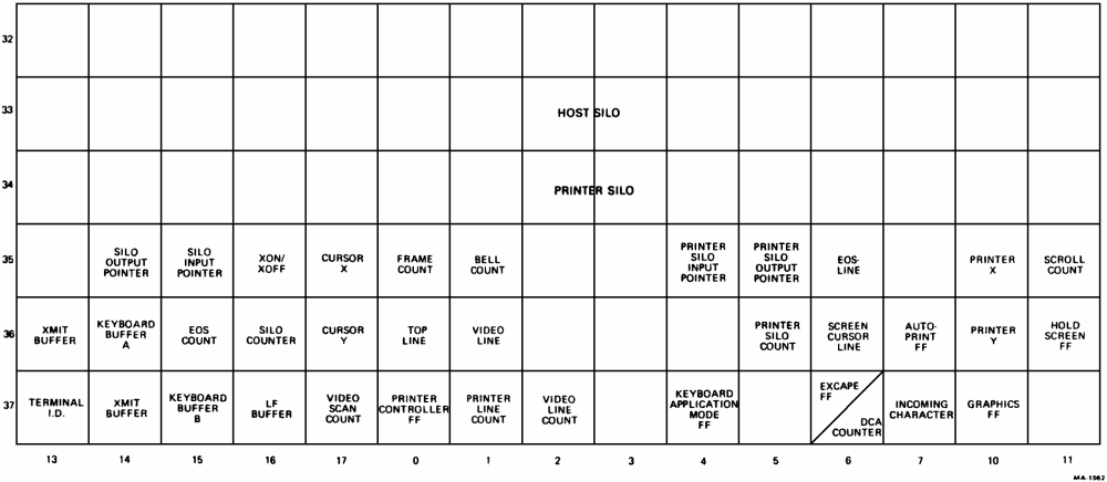
To perform all these tasks, the microprogram needs control registers and flip-flops, counters, temporary storage, etc. The scratchpad memory serves all these requirements. All VT52 status information is stored in the scratchpad. In addition, the scratchpad memory contains the silo used for storing incoming characters and provides temporary storage for keyboard characters. Figure 4-19 is a layout of the scratchpad memory.
Addressing the scratchpad memory is simple with the available microinstructions. Executing instruction ZXZY!DXDY will clear the X and Y registers and then decrement both registers, setting the Y register to 178, the X register to 1778, and selecting scratchpad location SCAN COUNT/KB COUNT.
Another instruction (X8) complements X register bit X3. This is the most significant X selection bit when addressing the scratchpad. Complementing this bit is like jumping eight X locations. Other instructions that increment or decrement the X and Y registers can be used to move around within the scratchpad.
Figure 4-20 is a flow diagram of the VT52 microprogram operations. Top-of-screen tests are performed at line frequency rates, i.e., 60 times each second in 60 Hz units; 50 times each second in 50 Hz units. The UART flag is checked after horizontal scans.
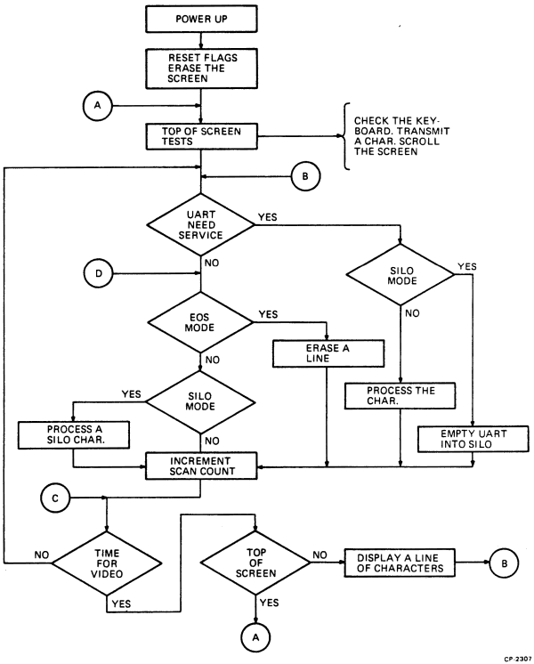
The keyboard is checked between displayed frames, i.e., during vertical retrace time. If one or more keys are pressed, the terminal transmits to the host the code representing the pressed key.
Figure 4-21 is a simplified flow diagram of the keyboard entry subroutine. The AC register is set to equal the highest numbered key on the keyboard and then a KEYJ command tests the flag to see if the key is down. If the key is not down, the AC register is decremented and the flag is tested again. This loop is repeated until a typed key is found. When an active key is located, the program stores the identification number of the key in the scratchpad memory. The program then looks up the ASCII code for the typed key in a table in the ROM, loads the ASCII character into the UART and transmits the character to the host.
If none of the keys are down, the program will exit the routine when the AC register is equal to zero. A jumper in the keyboard is wired to act like a typed key whenever it is referenced. It is referenced when the AC=0, meaning the keyboard was polled but no keys were down.
The identification number of the key is written into the scratchpad to prevent multiple transmission of the same character. Since the keyboard is polled 60 times a second, it is just about impossible not to detect a typed key more than once. As a first step then, the program reads the identification numbers stored in Keyboard A and Keyboard B of the scratchpad and checks the keyboard to see if these keys are still down. If they are, no transmission takes place during this scan. If one or both of the keys are up, the program clears the scratchpad location associated with the key and polls the keyboard.

A Line Feed (LF) command received from the host when the cursor is on the bottom line will cause the terminal to scroll. That is, every line on the screen will move up one position, leaving the bottom line blank, ready to receive more characters. Information displayed on the top line is lost and will be replaced by information previously displayed on the second line (line 1). To erase every RAM line and rewrite these lines with the contents of the following RAM line would take too much time and be an unreasonable way to accomplish scrolling, Instead, any RAM line can be displayed as the top line on the screen. This means that after one scroll the top line would be RAM line 1 and bottom line would be RAM line 0. Successive scrolls would cause RAM lines 2, 3, 4, etc. to be displayed as the top line and RAM lines 1, 2, 3, etc. to be displayed as the bottom line.
A scratchpad location is used to remember which RAM line is displayed on the top screen line. This location, TOP LINE, contains a line number between 0 and 23 and is cleared to 0 at power-up time. Memory location CUR Y contains the RAM line address of the cursor: location SCREEN LINE contains the screen line address of the cursor.
As an example, if the cursor is on line 5 and the top line is line 3, CUR Y will contain a 5 and SCREEN LINE will contain a 3; the cursor will be displayed on line 3 of the screen.
Hold-Screen mode allows the operator to control the rate at which data from the host enters and leaves the screen. If left unchecked, high-speed data from the host would be displayed for a very short time and then scrolled up and off the screen; the operator would not have enough time to read the data. In Hold-Screen mode, the terminal will avoid scrolling the display until commanded to do so by the operator.
When the cursor is on the bottom line of the screen and an LF command is received from the host, the program stores the Line Feed command in the LINE FEED BUFFER of the scratchpad and transmits the code for signal X OFF to the host. X OFF is used to request the host to stop transmitting data to the terminal. A few characters will be sent by the host before it receives and acts on the request. The program stores these characters in the silo portion of the RAM.
To request more data, the operator types SCROLL. The program responds by scrolling the screen and then processing the characters previously stored in the silo until the silo is empty. The program then sends X ON to the host and data transmission is resumed until another LF is received.
The silo portion of the RAM is addressed whenever the Y register contains 148. The X address of the silo is determined by two other locations in the scratchpad: SILO OUTPUT and SILO INPUT. SILO OUTPUT contains the X address of the next character to be processed by the terminal. SILO INPUT contains the X address of the first free silo location (the location where the next character will be stored). SILO OUTPUT = SILO INPUT when the silo is empty. When writing into the silo, SILO INPUT is incremented after each character is stored. When processing the silo characters, SILO OUTPUT is incremented every time a character is removed. SILO COUNTER, another scratchpad location, counts the number of characters stored in the silo; it contains the difference between SILO INPUT and SILO OUTPUT. As an example, assume the cursor is on the bottom line of the screen and an LF command is received from the host. SILO INPUT = SILO OUTPUT and we will assign address 2 to both of these registers. The LF command is stored in LINE FEED BUFFER and X OFF is sent to the host. If three characters are received before the data transmission stops, they will be stored in silo locations X2, X3, and X4. SILO OUTPUT will still contain 2 but SILO INPUT = 5 and SILO COUNTER = 3. When the characters are processed as a result of typing SCROLL, SILO COUNTER will contain a zero, SILO OUTPUT = SILO INPUT = 5 and the LINE FEED BUFFER will be cleared. If one of the characters in the example was an LF, it would not have been processed. Instead, it would have been stored in LINE FEED BUFFER and X OFF again sent to the host.
When the terminal receives the code for ESC Z from the host, it interprets this code as a request for the terminal to identify itself. The basic VT52 terminal does this by transmitting ESC/K to the host. A VT52 with copier option will transmit ESC/L; a VT52 with printer option will transmit ESC/M. The code for these three characters cannot be sent as one sequence; therefore, one character is sent after each frame displayed on the screen. The terminal must remember what portion of the sequence has been sent. Location ID of the scratchpad is used to store the status of the identification process. Five values are assigned to ID to indicate the different stages of the identification process. They are:
| 0 | An ESC Z command is not pending. |
| 135 | An ESC Z has been received. |
| 033 | Code for ESC has been sent to the host. |
| 057 | Code for slash (/) has been sent to the host. |
| 101 | Code for K (or L or M) has been sent to the host. |
During the identification process, the keyboard is not polled. This is to prevent keyboard characters from being mixed with the 3-character Escape Sequence.
When the last character in the sequence has been sent, location ID is cleared to 0 and keyboard polling resumes.
The cursor appears as a flashing underscore on the screen on the ninth scan of one of the 10 scan character rows. Although the screen is refreshed 60 times a second, the cursor display is refreshed only 4 times a second in order to produce a blinking cursor. To achieve this low frequency refresh rate, scratchpad location FRAME COUNT is preset to 160 and is incremented every time the Y line containing the cursor is to be painted on the screen. When FRAME COUNT overflows (every 15 frames), the CRT beam is turned on displaying the cursor, and FRAME COUNT is again preset to 160.