This section describes the contents of the technical description chapter and provides a technical overview of the terminal.
This technical description is intended to provide an understanding of the terminal operating principles for Field Service, depot repair, and engineering personnel. The description considers the terminal to be several functional or replaceable subunits. Each subunit is described in its own section. Several subunits interact. Those interactions are discussed in the section about the subunit most involved in the particular process. For example, power-up involves the nonvolatile RAM but is described in the microprocessor section. Scrolling has its own section because it is a complex process that involves the microprocessor and video processor equally.
Each section describes the hardware first and the associated firmware operations second. This section contains a block diagram level discussion of the terminal hardware and firmware. More detail is provided in the functional block descriptions in later sections. Refer to the VT100 series Field Maintenance Print Set, No. MP00633, for circuit details while studying this manual.
Many terms are written out the first time they appear, with an abbreviation or mnemonic in parentheses after it. The abbreviation is generally used after that. There is a glossary of abbreviations and signal names in the appendices of this manual. Numbers may be given in binary, octal, decimal, or hexadecimal (hex). The normal form will be decimal for scalar or ordinal values, and hex for data and addresses. Numbers are subscripted B for binary, Q for octal, H for hex, and no subscript for decimal.
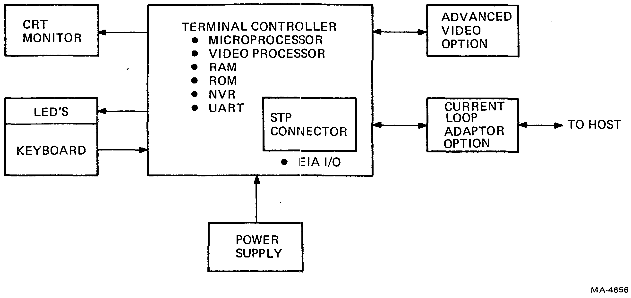
The VT100 is a complete computer input and output terminal that has a keyboard like a typewriter and displays its data on a video screen. It fits into two compact packages; the keyboard is flexibly attached to the main cabinet by a coiled cable. Refer to Figure 4-1-1.
The terminal consists of four basic components (not including enclosures) plus two important options. The components are the terminal controller, the keyboard, the CRT monitor, and the power supply. The options are the advanced video option and the current loop adapter option.

The terminal controller is a single pc board module that manages all displays and all communication. Everything else connects to it. The terminal controller contains these functional components:
The keyboard is the typewriter-style input device for the operator. It has a loudspeaker for user feedback keyclicks and bells, and indicators that show internal states of the terminal.
The CRT monitor is a video screen that displays exchanges between the operator and the computer. It can display data in two modes: 80 characters by 24 lines, or 132 characters by 14 lines (or, with the AVO, 132 by 24). With the control circuitry on the terminal controller board, the CRT can perform many special character display functions.
The power supply converts the ac power line to the four dc voltages required by the terminal. It has a switching regulator for highest efficiency and coolest operation.
The advanced video option provides greater display capacity, plus it can carry extra firmware for the expanded functionality of other products in the VT100 series.
The current loop adapter option converts the EIA output of the terminal controller to a more noise immune standard when longer distances between the terminal and the computer are required.
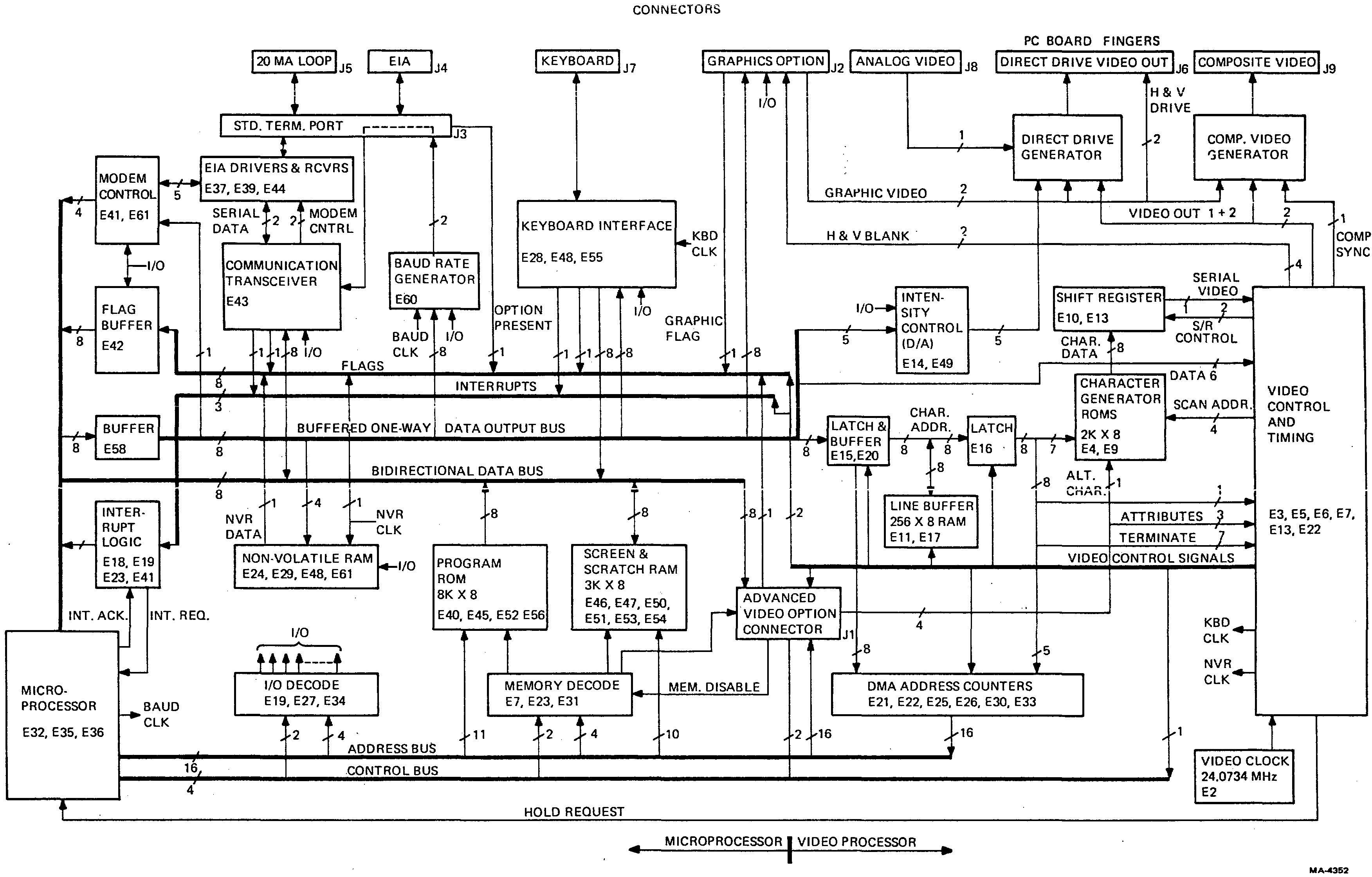
Figure 4-1-2 shows the VT100 terminal as a set of functional blocks. The rest of this section describes these blocks in greater detail.
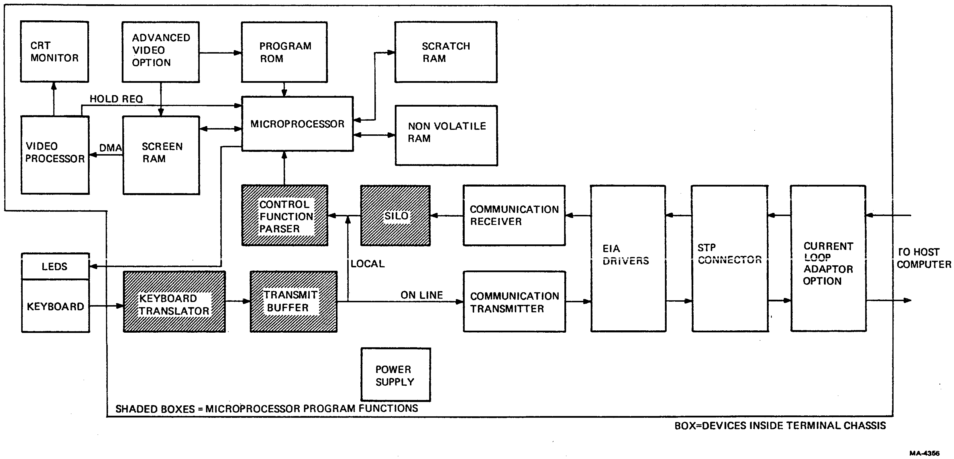
A microprocessor manages all terminal input and output operations. It also provides the intelligence that enables the VT100 to respond to and generate a wide range of ANSI control functions, and to emulate the characteristics of the VT52. Several of the microprocessor’s program functions are effectively in series with data paths in the terminal. These functions have their own blocks in the functional block diagram to clarify the processes involved. These blocks are shaded to indicate that they are program functions or that the microprocessor controls data transfers between the blocks. The microprocessor is a computer with its instructions in program ROM (read only memory) and working memory in the scratch RAM (random access memory). Terminal parameters for start-up are stored in the nonvolatile RAM (NVR). The advanced video option (AVO) normally contains extra RAM as described below but can also contain extra program ROM.
The VT100 program ROM is an 8K × 8 memory containing instructions and data tables for the terminal’s microprocessor. Memory comes in four 2K packages (later VT100s may have a single 8K package). Checksum data stored in each ROM allows the terminal to confirm the condition of its programming at self-test.
The scratch RAM is the portion of RAM on the terminal controller that is not used for the screen RAM. That is, the RAM is 3K bytes long, but only about 2.3K bytes are used for screen display. The rest of the RAM contains the microprocessor stack, SET-UP data, various flag bytes, the communication SILO, the keyboard buffer, and so on.
The nonvolatile RAM (NVR) does not lose its data when its power is off. It stores all user-settable features and parameters and the answerback message so that they are available each time the terminal is turned on. Even the screen intensity can be stored. There are no mechanical switches needed for configuration.
The advanced video option (AVO) contains the 1K × 8 of extra screen RAM needed to expand the display from 14 lines of 132 characters to 24 lines, plus a 4K × 4 RAM to store an extended set of attributes for all characters. The AVO also contains an additional segment of video processor to manage the four extra bits of data. Sockets for ROMs and jumper- or switch-programmable decoders allow expansion or overlay of program memory.
The AVO is a replaceable subunit of the VT100.
The keyboard is the user’s input device to the terminal. The keyboard’s output is a serial data signal that travels along the same wire as data coming from the terminal. The keyboard contains a bidirectional interface circuit, a set of keyswitches arranged like a typewriter, circuits to send the key information to the interface, LED indicators, and a small loudspeaker for keyclicks and bells. The connection to the terminal is a 3-wire coil cord carrying signals, power, and ground.
The keyboard is a replaceable subunit of the VT100.
The terminal can inform the user of some internal conditions such as on-line or local and keyboard locked through the LEDs on the keyboard. The LEDs also may indicate the location of a failure during self test and are user programmable during normal operation.
The output for each key is a number that represents the key’s location (address) in the keyboard switch matrix. The microprocessor’s keyboard translator translates the address to the industry-standard ASCII code.
The ASCII codes wait in a transmit buffer until they can be transmitted. Some keys (such as the numeric keypad in application mode) produce control functions that are three bytes long. The transmit buffer is nine bytes long and thus can store at least three keys of any kind.
The communication transmitter is one-half of a programmable universal synchronous/asynchronous receiver transmitter (PUSART) and its associated circuitry and firmware routines. The PUSART is programmed to place data in a standard asynchronous format by adding control and error detection bits to the original byte. The communication transmitter thus takes the parallel ASCII keycodes out of the keycode buffer, converts them to serial form, and delivers them to the EIA interface.
Data that the host sends to the terminal enters the communication receiver which is the other half of the PUSART. The PUSART accepts serial data from the interface and converts it to parallel form. The PUSART also checks for errors and records them in a status byte. The microprocessor reads the data and then the status byte to confirm the correctness of the data. If an error is detected, a checkerboard is displayed instead of a character to symbolize the error. If the microprocessor is busy managing the display, it devotes only enough time to the communication receiver to get the incoming code and check it for special codes requiring immediate action.
The rest of the incoming codes are stored in a part of RAM memory called a SILO. This memory maintains the order of the data as it arrives; the first data to arrive leaves first. This memory gives incoming data a place to wait when the microprocessor cannot transfer data from the communication receiver to the screen RAM as fast as it arrives. The SILO control routine checks the filling of the SILO and can issue XON and XOFF commands to the host to try to keep from overfilling. (XON and XOFF are explained in Section 4.3, Communication.)
In local mode, data from the keyboard bypasses the communication receiver and transmitter and the SILO.
When the microprocessor has enough time, it takes data from the SILO and puts it through a control function parser routine in the microprocessor. Each code is tested to see if it is in the control range (<20H or 7FH). If it is, the microprocessor acts on it immediately. Line feed, for example, causes a one line scroll. If the code is 1BH (escape), more codes are read from the SILO until the characters that define a control function are seen. Then the microprocessor executes the control function immediately or discards it if it is not a valid function. Noncontrol codes are ignored by the parser and are written into the screen RAM.
The screen RAM is a memory that stores data for display on the screen (CRT monitor). The memory is organized according to the SET-UP line length specifications. Basic terminal memory can hold 24 lines of 80 characters or 14 lines of 132 characters. With the extra memory provided by the advanced video option, the screen size may increase to 24 lines of 132 characters and four additional bits are appended to each character location to allow expanded character attributes. (A character attribute modifies the display of that character relative to the preset values for the entire screen.)
Most of the time, the screen RAM is readable and writable by the microprocessor. For about 10 percent of the time, during the first scan of each 10 scan line of characters, the video processor silences the microprocessor and takes full control of the screen RAM, providing its own addresses to access the memory. This complete control of memory (by a device other than the microprocessor, which is normally in control) is called a direct memory access (DMA). The DMA allows fast access of data in memory because the microprocessor does not have to perform all the steps of addressing, reading, and writing to a destination. The video processor needs the fast access because the data rate required to display a line of characters on the CRT is greater than the microprocessor can handle.
The microprocessor puts displayable data in the screen RAM, The video processor direct memory accesses (DMAs) data a line at a time from the RAM. It converts the ASCII-encoded data into streams of pulses which, when converted to light on a CRT screen, appear to form characters on the screen. Custom ICs provide the complex timing and control signals required for this conversion. The video processor can be programmed by the user to perform the conversion at different rates (called refresh rates) to minimize flicker at different power line frequencies. A number of other aspects of video processor operation can be programmed as well.
The cathode ray tube (CRT) monitor is a simplified monochrome television set. It converts electrical pulse streams into dots of light by exciting a phosphor on the face of the tube with a moving electron beam. A video input from the video processor enters a cathode drive circuit that regulates the strength of the electron beam. The cathode driver is a linear amplifier that allows the CRT to display different intensities (gray scale). The monitor uses timing pulses from the video processor to drive the horizontal and vertical electron beam deflection circuits. These circuits cause the beam to travel down the screen slowly while rapidly moving sideways to draw horizontal traces called scans. This beam movement produces a pattern which is called a raster and the display system is called raster scanning. Because the beam repeatedly passes by each location on the screen, the video processor, by synchronizing its output with the motion of the beam, can make rows of dots of light align to form characters.
The screen does not hold its image after the electron beam has painted dots on it. For the eye to perceive it as continuously illuminated (i.e., without flickering) the screen must be repainted (refreshed) repeatedly some 30 or more times per second. Also, stray magnetic fields and electrical noise at the power line frequency can cause distortions in the display. If the refresh frequency is different from the power line frequency, the distortions appear to move up or down the display. This is very noticeable. Most distortions disappear by matching the refresh rate to the power line frequency. The VT100 can refresh at either of the two world power frequencies, 50 or 60 Hz, satisfying both flicker and distortion requirements. (VT100 refresh is not locked to the power line but is close enough to conceal most distortions.)
The CRT monitor, the monitor circuit board, and the flyback transformer are replaceable subunits of the VT100.
The VT100 power supply provides enough power to run the terminal and a few options. It is a switching supply to allow highest efficiency and to minimize the heat load on the rest of the terminal. It rectifies line voltage directly (without a transformer), and chops the resulting high dc voltage with a transistor at about 30 kilohertz. This ultrasonic ac is stepped down in a relatively tiny transformer and then regulated at low voltage to give the various outputs.
The power supply is a replaceable subunit of the VT100.
The standard terminal port (STP) is a shorting connector in series with the communication port, the modem control lines, and some power and timing lines. By connecting to the terminal through this port, options can exchange signals with the terminal controller or intercept terminal-host communications from inside the terminal cabinet.
The Electronic Industries Association (EIA) interface used on the VT100 is the RS-232-C unbalanced bipolar voltage standard. The terminal controller has two types of ICs that provide conversion between EIA levels and the TTL levels used on the controller board. One IC is a line driver that outputs EIA levels for TTL inputs, and the other senses the EIA levels on the input line and converts them to TTL.
The current loop adapter option plugs into the terminal controller board and mates with the EIA voltage interfaces to convert the terminal to 20 milliampere current loop interfaces. The current loop interfaces can be individually selected to be active or passive.
The 20 mA adapter is a replaceable subunit of the VT100.
Figure 4-1-3 portrays the VT100 as a system with four levels of operation.
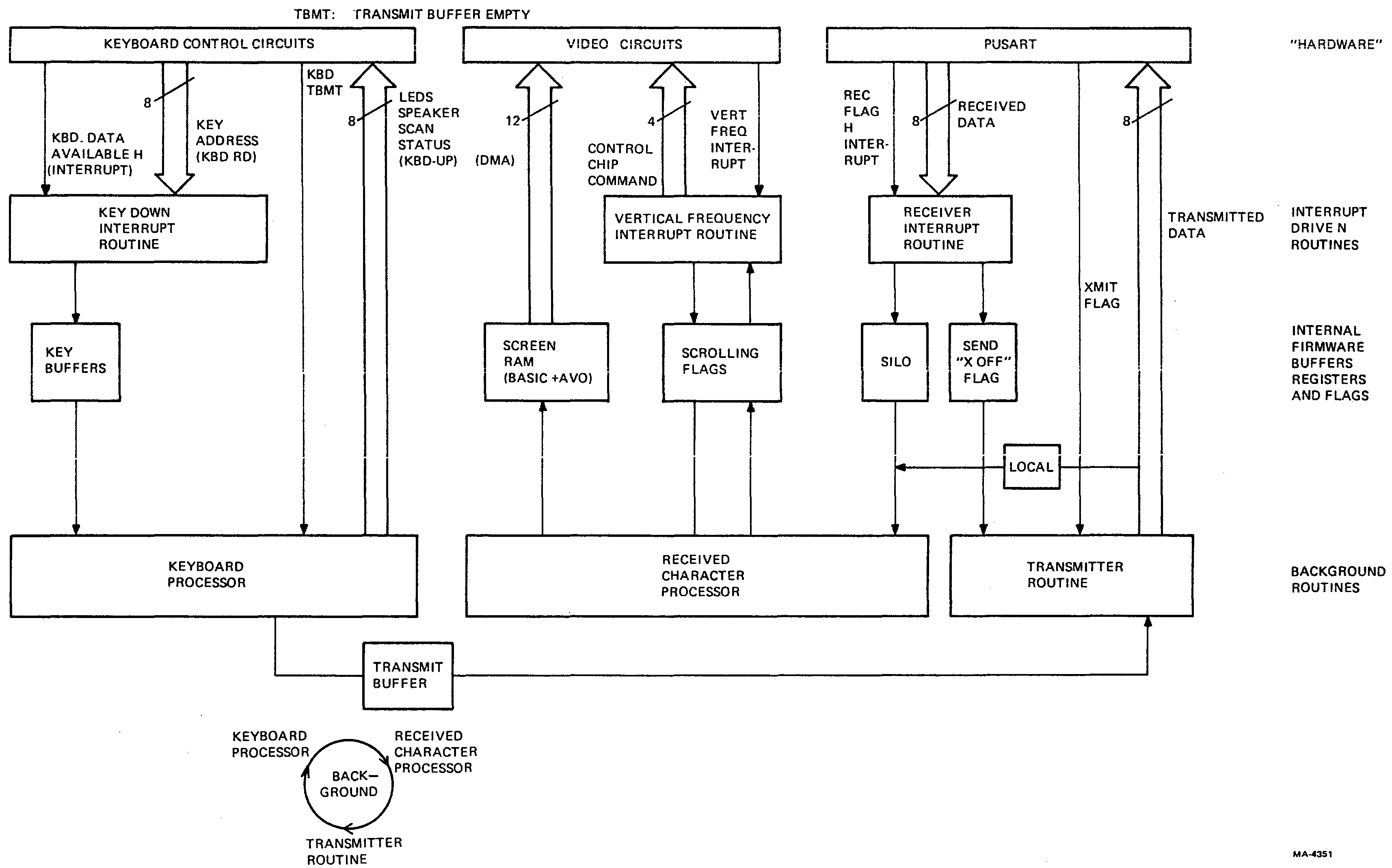
At the deepest level, the background routines continually repeat to manage functions that do not require precisely timed responses. The keyboard processor commands the keyboard to perform address scans, controls the bell and LEDs, and manages the conversion of key information from hardware-dependent codes to ASCII. The transmitter routine manages the transmission of ASCII data to the host. The received character processor examines incoming data, manages the SILO, initiates special functions as specified in the data, and writes displayable data into the screen RAM. When the terminal is in local mode, a logical shortcut bypasses the communication process and allows the keyboard data to enter the received character processor directly.
The background routines work on the internal buffers, registers, and flags which are logical devices located in hardware and RAM. These are physical locations in hardware that contain information placed there by the hardware and by the firmware. The key buffers store up to three key addresses for the keyboard processor to pass through the transmit buffer to the transmitter routine for transmission to the host. The screen RAM, which stores the displayable data, is the largest segment of RAM. The scrolling flags contain data for the scrolling process in the video processor. The SILO stores data coming from the host in case the received character processor cannot transfer data to the screen RAM as fast as it arrives. The Send XOFF flag, set by the SILO manager, signals the transmitter routine to send the XOFF code to the host to halt transmission and prevent SILO overflow.
Interrupt routines are segments of the firmware that take precedence over other business in the microprocessor because of the short-lived nature of the data that they handle. The Key Down interrupt routine is initiated by the appearance of data at the keyboard control circuits. It instructs the microprocessor to get the key address from the keyboard UART and put it in the key buffer. The Vertical Frequency interrupt routine occurs every 50th or 60th of a second and provides synchronization of video routines with the actual display timing. The Receiver interrupt routine moves incoming data from the communication transceiver to the SILO.
At the exterior level of the VT100 system, the hardware responds to the firmware by exchanging data between the user and the host computer in forms that are understandable to each.
The VT100 has an 8080 microprocessor at the heart of its intelligence. The 8080 performs all the usual functions of a stored program computer, fetching instructions and data from ROM and RAM and responding to service requests from various devices in the system. Because of technical limitations in the implementation of the microprocessor hardware, some high speed counting and timing circuits and some power circuits are located in peripheral ICs made with a different semiconductor technology. These components are bipolar (8224, 8228) while the 8080 is NMOS.
The 8080 (Figure 4-2-1) contains a set of general and special purpose registers (the register array), timing and control logic which responds to machine code instructions, and an accumulator and arithmetic logic unit that perform the computations associated with the microprocessor operation.
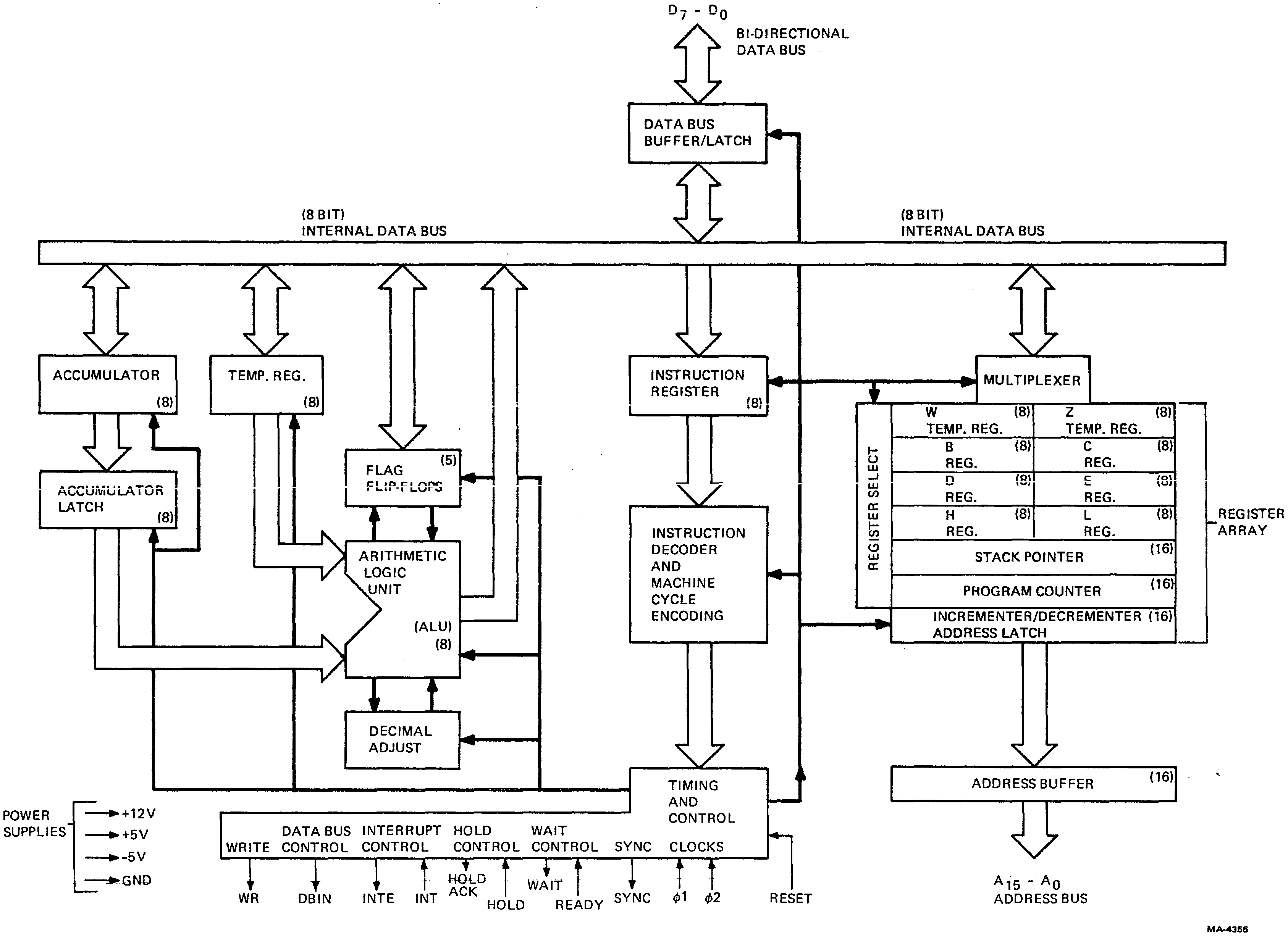
The stack pointer is an important register that points to the bottom of the stack. The stack is a last-in/first-out area in RAM that stores information about the current process when a subroutine or interrupt branches away from the current instruction sequence. By storing this information at the beginning of an interruption and restoring it at the end of the interruption, the 8080 can continue the main program without any disturbance. This is the meaning of the interrupt process as it applies to the interrupt-driven routines mentioned in the firmware block diagram in Figure 4-1-3.
Most of the pins on the 8080 are tristate data and address lines. Four pins are power supplies and ground. The others, briefly, are:
For more detail, see Intel’s 8080A manual.
The microprocessor data bus passes directly to the 8228 bus driver and system controller. This device provides TTL output buffering and level translation for the MOS 8080 bus. Because of the large number of devices on the data bus, the drive capability of some devices would be exceeded at times if all devices were on the same bus. (The keyboard UART is the weakest low-level current driver.) To distribute the load, the bus is split into those devices that communicate bidirectionally or are only read by the microprocessor, and those that are only written into. Read and writable devices are on the bidirectional data bus (DB). The write-only devices are driven by a one-way bus buffer and are on the data output (DO) bus. The terminal controller block diagram (Figure 4-2-2) shows which devices are on each bus.
The ROMs do not have sufficient high-level current capacity to drive all of the other inputs on the bus. Inactive devices have their outputs tristated but their inputs still draw enough current to accumulate a significant load over the entire bus. Pull-up resistors are connected to the bus to provide the additional current required. Their resistance is selected to supply enough current to meet high level needs on the bus without exceeding the low level sink capacity of any driving device.
Pull-up resistors are used on the output-only DO bus because the baud rate generator, a MOS device, has an input threshold higher than TTL driver E58 is guaranteed to deliver. Pull-up resistors ensure that the data lines rise enough.
An additional function of the 8228 is a combinational logic decode of the 8080 status byte. This byte, output by the 8080 at the beginning of each machine cycle, contains flag bits indicating the nature and function of the cycle. The byte is latched into the 8228 by the Status Strobe (STSTB) signal from the clock generator. In combination with three control output bits from the 8080, the system controller produces Interrupt Acknowledge (INTA) and Memory and Input/Output Read and Write (MEM WR,RD; I/O WR,RD). These signals reduce the external decoding requirements while saving pins on the 8080 package.
When the video processor asserts Hold Request during a direct memory access (DMA) of the screen RAM, the 8228 floats its outputs. Since these include the memory control signals, the video processor must provide its own memory control. The DMA Enable signal, buffered into the MEM RD line by gate E28 (pin 13), provides memory read enabling during the DMA. The other control signals are pulled high by the pull-up resistors.
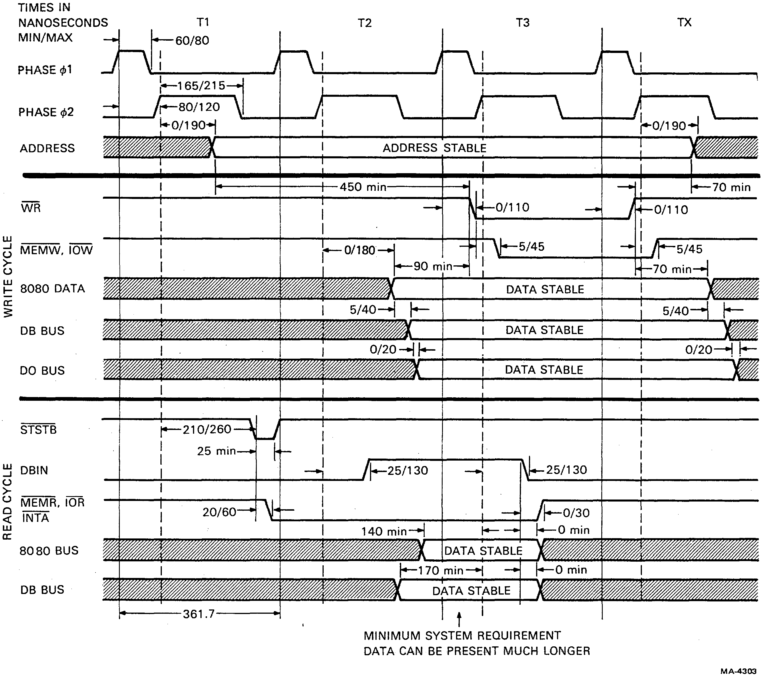
The 8224 provides the asymmetrical two-phase clock required by the 8080 logic. Its running frequency is crystal-controlled. An LC circuit on the tank input improves the crystal’s mode stability. The capacitor in series with the crystal compensates for internal phase shifts in the 8224 at the high operating frequency. The 24.8832 MHz crystal frequency gets divided by 9 to produce a 361.69 ns clock period. The buffered TTL phase 2 output clocks the PUSART and the baud rate generator. 361.69 ns is the system clock period for the microprocessor.
The sync signal from the 8080 combines with an internal clock phase to produce the Status Strobe (STSTB) during the last ninth of the first state of each machine cycle. STSTB latches the status byte into the 8228 system controller.
The Ready input is not used in the VT100. It is an asynchronous input that gets synchronized to the machine cycles in the 8224. The synchronized signal can cause the microprocessor to enter a wait state during a memory access to wait for slow memory to respond. Memory used in the VT100 matches the processor speed so Ready is not used.
The Reset input is a Schmitt trigger. Its input is the +5 volt supply delayed by an RC circuit with a diode bypass for fast discharge. The Reset input is held low until well after all power supplies have settled. When the capacitor voltage reaches the Schmitt threshold, reset is released and the microprocessor begins operation at memory location 0 (the start of the firmware ROM). The inverted and noninverted reset signals clear other portions of the terminal controller.
The bus timing diagram in Figure 4-2-3 illustrates the basic time relations between the address, data, and control lines in the microprocessor system. The figure distinguishes between write and read cycles, with the exception of the three top lines. These show the constants of the system: the two clock phases from which all timing is derived, and the address bus, that always provides the current address for either kind of cycle early in the cycle. Numbers on the diagram represent specified minimum/maximum nanoseconds between signals for normal operation.
Starting with the write cycle, note that the status strobe signal (STSTB L) shown in the read section occurs at the same point in the write cycle. Therefore, the status strobe latches the status byte into the 8228 during the first clock cycle. The 8228 delivers the decoded Memory Write L or I/O Write L (MEMW or IOW) signals in the third clock cycle when data to be written is stable. The 8080 Data Bus, DB Bus, and DO Bus graphs show the propagation delays between the three buses. The 8080 bus is the output pins on the chip. The DB bus is the output of the buffered 8228 bidirectional bus, and the DO bus is the unidirectional buffered output-only bus.
In the read cycle, the Memory Read L signal (along with I/O Read L and Interrupt Acknowledge L: MEMR, IOR, INTA) starts early to enable the chip selects and allow the data buses to stabilize. Data Bus In (DBIN) goes high before data settles but does not latch data into the 8080 until its falling edge, when data is settled. The two bus graphs show the assertion of stable data and also show the delay through the bidirectional bus buffer to the 8080 data bus.
The basic terminal controller contains 8192 bytes (8K) of program ROM and 3072 bytes (3K) of static RAM. (One byte = eight bits.) The original board utilizes four 2K × 8 ROM ICs; later versions may use a single 8K × 8 ROM. The RAM is six 1K × 4 ICs arranged in pairs. The microprocessor can address up to 64K memory locations. Some of these locations are reserved for future expansion. The memory map of Figure 4-2-4 shows the portions of addressable space that are reserved and also those areas that are available for new applications.
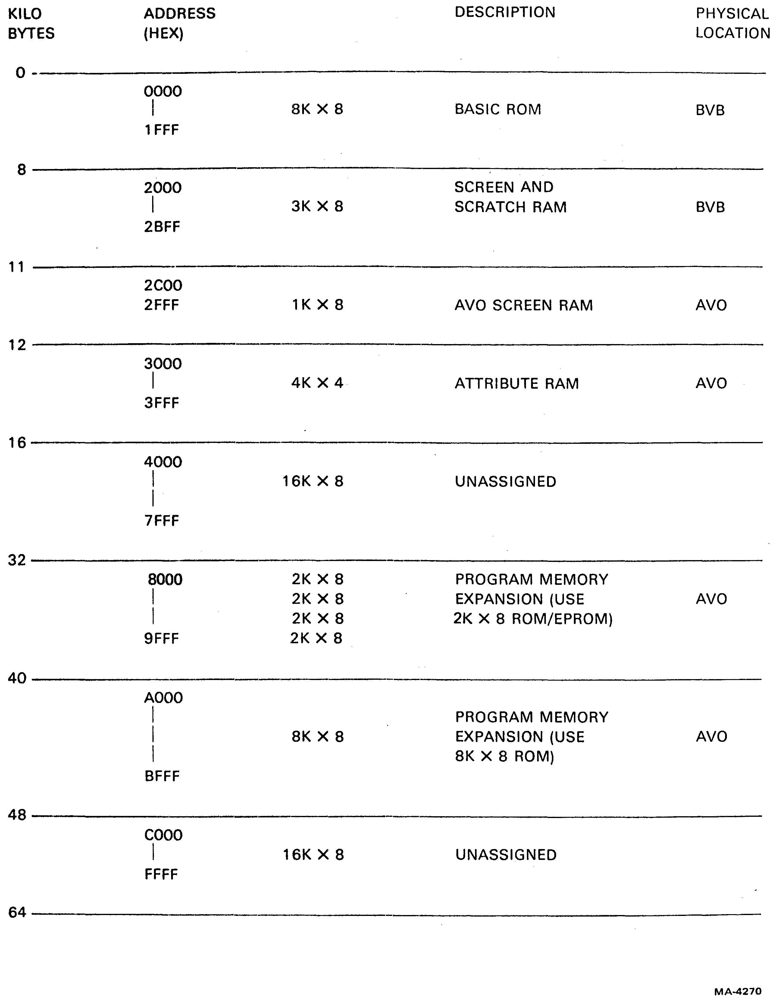
The basic terminal controller board contains 8K of program ROM and 3K of screen and scratch RAM. These account for the locations from 0000H to 2BFFH in memory. The advanced video option adds another 1 kilobyte of RAM (2C00H to 2FFFH) to increase the number of characters that can be displayed. The AVO also contains additional memory for character attributes. This memory is only 4 bits wide, but to address each location in correspondence with each of the 4K characters, it uses another 4K of addresses from 3000H to 3FFFH.
The next 16K locations (4000H to 7FFFH) are unassigned. However, 4000H to 4FFFH can be addressed by the video processor using the DMA address counters so 4000H to 4FFFH could be used for additional screen RAM with 5000H to 5FFFH as associated attribute storage.
Above 7FFFH is an 8K area intended for additions or changes to the program ROM in 2K segments and above that is an area intended for the same purpose but in one 8K segment. The top 16K are unassigned.
Each ROM has three ANDed chip select inputs that are mask-programmed to be either active-high or active-low, eliminating the need for external inverters. The programming provides 1 of 4 decoding of the two address lines A11 and A12. The third chip select line is common to all four ROMs. In later VT100s jumpers W2 and W3 can be used to select either a high or low assertion for this single chip select to allow for 64K ROMs that do not have a programmable chip select. Table 4-2-1 shows the addressing of the ROMs.
| Address Line 11 | Address Line 12 | Chip Select 2 | Chip Select 3 | ROM Selected |
|---|---|---|---|---|
| 0 | 0 | Active Low | Active Low | 1 |
| 1 | 0 | Active High | Active Low | 2 |
| 0 | 1 | Active Low | Active High | 3 |
| 1 | 1 | Active High | Active High | 4 |
The program ROM is enabled when the top half of memory decoder E31 is enabled and the correct address space is requested by the microprocessor. MEM RD or MEM WR from the 8228, in the absence of MEM DISABLE, enables the decoder. The ROM is in addresses 0H to 1FFFH, so A13 (the 8K bit) is not asserted during ROM reads. Bit A12 is low or high for 0-4K or 4-8K sections of ROM. The decoded outputs from both states are ORed to provide one of the select signals for the ROM. Then bits A11 and A12 at two of the chip select lines enable the outputs in one of the 2K segments. The low 11 bits address one of the 2K bytes in the enabled ROM. If the program is in one 8K ROM, A11 and A12 are used as regular address lines; only one chip select line enables its outputs.
If A13 is asserted, the memory space between 2000H and 3FFFH is being addressed. The ROM outputs are disabled and the decoded output from the top half of the decoder enables the bottom half. Now bits A10 and A11 are decoded to select 1K segments of the screen RAM. The 1K × 4 RAMs are paralleled in pairs to make each location 8 bits wide. There is 3K on the basic video board. The fourth 1K is located on the AVO; its addressing is decoded separately.
Memory Disable turns off all memory on the terminal controller board. It is used by options that plug into the advanced video option connector:
The advanced video option can contain overlaying program memory. This is a set of address locations that the AVO can be jumper-programmed to decode and provide data for. Since the main memory may also be decoding the same location, the AVO must assert MEM DISABLE to disable the main memory (ROM and RAM) so that only one data byte is asserted on the bus.
The I/O address space is divided into two regions: one, containing the 8251 PUSART, has address bit A01 always low; the other region contains all other I/O devices and has bit A01 always high. The list of I/O addresses in Table 4-2-2 illustrates this by the presence of hex 2 in the low half of each non-PUSART address byte.
| READ OR WRITE | |
| 00H | PUSART data bus |
| 01H | PUSART command port |
| WRITE ONLY (Decoded with I/O WR L) | |
| 02H | Baud rate generator |
| 42H | Brightness D/A latch |
| 62H | NVR latch |
| 82H | Keyboard UART data input |
| A2H | Video processor DC012 |
| C2H | Video processor DC011 |
| E2H | Graphics port |
| READ ONLY (Decoded with I/O RD L) | |
| 22H | Modem buffer |
| 42H | Flags buffer |
| 82H | Keyboard UART data output |
When bit A01 is low, the PUSART is enabled. The I/O RD and WR signals from the 8228 control the read or write operation. Address bit A00 selects either the command or data register for the I/O operation.
When bit A01 is high, the PUSART is disabled. Bit A01 high is one of two signals required to enable the I/O write decoder (E27). I/O WR is the other signal. Address bits A05, A06, and A07 select one of the seven writable I/O devices. These are the baud rate generator, the brightness control D/A latch, the NVR latch, the keyboard UART transmit buffer, the DC011 and DC012 video processor chips, and the graphics processor data port.
Only three I/O devices are readable so their addresses were chosen to allow read decoding directly from the three address lines. When the 8228 asserts I/O RD, I/O WR deasserts and decoder E27 is disabled. I/O RD enables the gates in E34 to allow reading of the keyboard UART receive buffer, the flag buffer, or the modem control signal buffer, depending on which address bit is asserted.
When any of the three interrupting devices (communication receiver, vertical frequency, or keyboard) sets Interrupt Request (INTR H) through gate E23, the current instruction is completed and then the microprocessor sets its Interrupt Acknowledge (INTA) status bit and performs an instruction fetch. The address requested in the fetch is the contents of the program counter. Its value is ignored in the interrupt process, but it is not incremented, as it would be in a normal fetch cycle. The INTA bit is decoded from the status word in the 8228 system controller; it enables the tristate interrupt vector buffer (E41) which then presents a restart (RST) instruction to the data bus. Main memory does not conflict with the vector buffer because the 8228, in decoding the interrupt status word, does not produce the memory read or write command bits needed for address decoding. (Refer to Table 4-2-3.)
| 00H | Power-up (Not hardware driven) |
| 08H | Keyboard |
| 10H | Receiver |
| 18H | Receiver and keyboard |
| 20H | Vertical frequency |
| 28H | Vertical frequency and keyboard |
| 30H | Vertical frequency and receiver |
| 38H | Vertical frequency, receiver and keyboard |
The RST instruction disables further interrupts, pushes the current program counter contents (the location of the next instruction in the interrupted program) onto the stack and decrements the stack pointer. Then the program counter is loaded with the bits in the address field of the RST instruction. This field is produced by the interrupt signals of the interrupting devices. The signals are passed onto the data bus as bits in the address field (bits 3, 4, and 5). The rest of the instruction is hard-wired through diodes that supply high level to the other data bits during INTA and that are reverse-biased to isolate these data bus lines when the vector buffer is inactive.
The RST address field, when mapped into the same bit locations in the program counter, defines a set of eight 8-byte long memory spaces at the beginning of the memory. The first address, 0, is the starting point for the terminal controller program and is not used for interrupts. The program is normally started by a hardware reset signal that sets the program counter to 0. It can also be started by an escape sequence that the host can send to force the program to jump to zero, or in SET-UP mode the RESET key can be pressed. The other seven memory spaces, starting at 8, 16, etc., contain jumps to places in an interrupt handling routine that can mediate requests for service from any of the seven combinations of interrupting devices.
At the end of the interrupt service routine, the stack is popped, interrupts are enabled, and the interrupted program continues.
Early VT100s can disable the receiver interrupt by programming D4 in the NVR latch. However, this is never used by the VT100. Later VT100s instead, have the ability to add a Communications Transmit Buffer Empty interrupt by adding W6. The 8080 would then have to distinguish transmit and receive interrupts by testing the transmit flag on the flag buffer. This provision is not used on the VT100.
When power is first applied to the terminal controller board, the reset circuit in the 8224 holds the microprocessor in a halt state. Within a second, after the voltages stabilize in the power supply, the RC network at the reset input allows the input voltage to rise to the switching threshold of a Schmitt trigger. Then the reset is released with the 8080 program counter set to 0. The low 64 bytes of program are reserved for the eight interrupt service routines which can be addressed by the restart instruction (see previous section). The low 8 bytes start the power-up routine by disabling the interrupts, setting up the stack pointer, and then going immediately into the self-test routines.
Assuming there are no hard logic failures present on the board, the microprocessor attempts to perform a confidence check of the controller. Some failures are considered fatal and will stop the machine; other failures limit its operation but will not prevent its use. Fatal failures are indicated by the LEDs on the keyboard, while nonfatal errors are indicated as a single character on the screen.
The microprocessor first sends the number of the first ROM to the LEDs on the keyboard. Then it calculates a checksum of the contents of the first 2K of program. (Since firmware is treated as four 2K blocks of code, later VT100s with one 8K × 8 ROM chip operate the same way but any block failure requires replacement of the one chip.) At the time of ROM preparation, a special byte was included within each block to make the checksum equal zero if there are no errors. If there is an error, the microprocessor halts and the LEDs indicate the current ROM at the time of failure. Otherwise, the LEDs are incremented to show the next ROM number and the process continues.
The next part of the test is writing and reading the RAM. Every bit in the RAM is written with a 0 and a 1 and read each time. If the advanced video option is present (as indicated by the Option Present flag), its RAM is tested immediately after the main RAM. In the main RAM a failure halts the machine. Failure of a bit in the advanced video option RAM is indicated on the screen and the process continues. In another terminal, like the VT52, one bad bit in the screen RAM means there is one location that may not contain the right character. This can be annoying to the user but does not affect the rest of the screen. If one bit is bad in a VT100 line address, the entire screen below the affected line can become garbled and unusable. A bad bit in the scratch area could disable communication with the host. So this confidence check ensures that any RAM failure is detected immediately.
The next test checks the nonvolatile RAM by reading it. A checksum is calculated and compared with the value stored the last time the NVR was written during a save. A bad NVR does not stop the VT100 because the SET-UP values can always be reestablished from the keyboard at power-up. The NVR test is also the normal time when the terminal gets its auto SET-UP readings from the NVR. Time is saved because reading the NVR is the most time-consuming part of both the self-test and the auto SET-UP. If the NVR fails, the bell sounds several times to inform the operator, and then default settings stored in the ROM allow the terminal to work. The operator must then manually reset any parameters that differ from the default values.
To test the keyboard, the microprocessor commands the keyboard to scan once, lights all the LEDs, for about a half second, and sounds the bell. It waits for the scan to finish and then looks for the last key address 7FH at the keyboard UART. If the test fails, the terminal remains on-line, making it a receive-only (RO) terminal.
This is the end of testing.
Once the NVR data is in the scratch area in RAM, the microprocessor uses that data to program the hardware. All operating parameters that were last saved (see NVR) are recalled and the terminal is set to match them. Finally the cursor appears at column 1, line 1, and the microprocessor enters its background routine, ready for operation.
Refer to the Communication chapter for a discussion of Data and EIA tests, and to the Service chapter for a listing of the Self-Test Results tables.
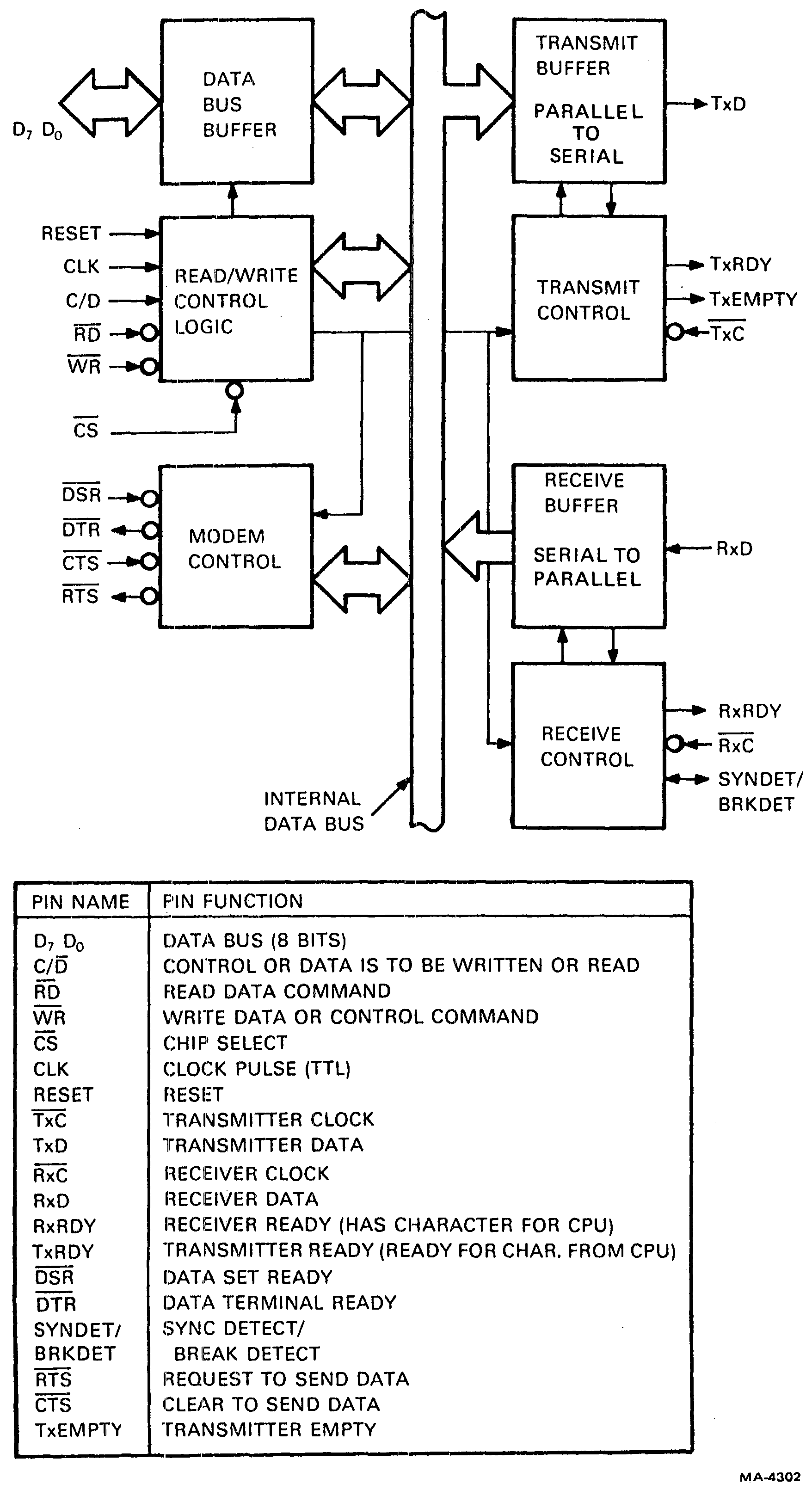
The VT100 interfaces to its host system through a serial data port. An 8251 programmable universal synchronous or asynchronous receiver-transmitter (PUSART), illustrated in Figure 4-3-1, drives the port. This device translates between parallel and serial formats, adding or removing start and stop bits as required. The data exchanged are ASCII characters; parity may be enabled or disabled; the selectably odd or even parity bit will take the most significant bit position.
Most data in computer systems is exchanged as groups of bits. The bit is the smallest unit of information, but to be useful, most information must be encoded into groups of bits in standardized patterns. The VT100 operates with the standard patterns described by the American Standard Code for Information Interchange (ASCII). ASCII defines the use of 7 bits, specifying 128 different patterns that correspond to almost all of the letters, numerals, and punctuation marks used in English and several other languages. An eighth bit is reserved for an expanded standard.
The eight ASCII bits can be exchanged most rapidly over eight separate wires (in parallel), but this is very expensive to do anywhere outside the computer cabinet. Instead; the bits are rearranged to pass over a single wire one after the other. This is called serial transmission. The circuitry for converting parallel to serial and back again is complex but suited to large scale integration (LSI). The savings allowed by the use of serial lines has encouraged the development of very sophisticated but inexpensive conversion devices in LSI. At the same time, a variety of data exchange protocols has been developed. The result is an LSI device that can operate with virtually any protocol depending on the programming that it receives from its local processor. This is the PUSART. The VT100 uses one such device (Intel’s 8251A) only in asynchronous mode, plus two simpler, wire-programmed asynchronous-only UARTS for the keyboard interface.
Synchronous and asynchronous describe the manner in which separate groups of bits (called bytes) are exchanged. In order for a receiver to know which bit is arriving at any given time, it must know the format of the byte and which bit of the byte is the first one. In synchronous mode, one or more special bytes are transmitted which the interface recognizes as synchronizing characters. Then all data bytes are transmitted together in rapid and precisely timed succession. Both the transmitter and receiver must have the same externally-supplied clock.
The VT100 only communicates asynchronously. Asynchronous transmission uses bits added to each data byte to provide synchronization between the transmitter and receiver. Because any two data exchanges can originate at random times with clock frequencies as much as 1 percent different, the protocol assumes random arrival of any byte of data, and relies on the synchronization information in the byte. This synchronization consists of extra bits appended to the beginning and end of the byte. One bit at each end (one start bit and one stop bit) is the most common configuration. The start bit and stop bit are defined to have specific states, and in particular, the start bit has a different state from the idling condition on the line. The interface looks for the transition from the idling state (called mark) to the start bit state (called space) and then clocks in the byte. The stop bit is the mark state, as is the idling line, so an immediately following byte has the correct mark to space transition to provide synchronization. The data bits, which occur between a start and a stop bit, are represented by a mark for a one and a space for a zero. Figure 4-3-2 shows the asynchronous data format.
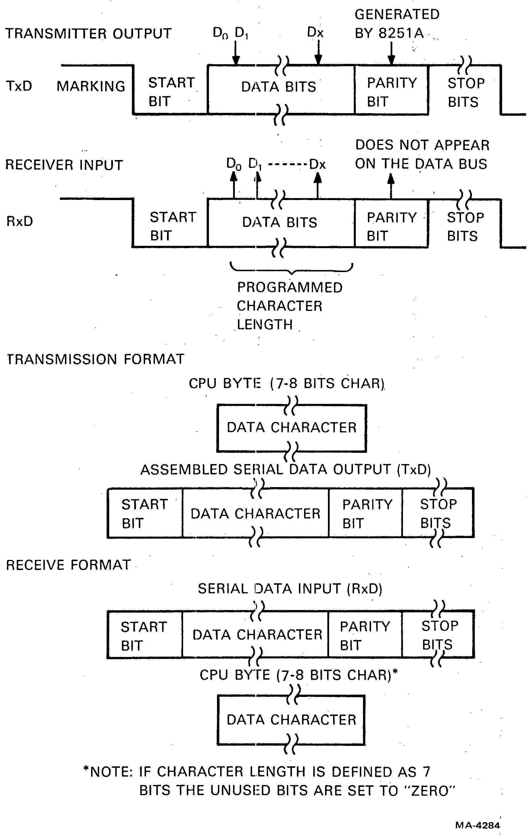
The complete functional definition of the PUSART is programmed by the system’s software. A set of control words must be sent out by the microprocessor to initialize the PUSART to support the desired communications format. Once programmed, the PUSART is ready to perform its communication functions. The Transmitter Ready (TxRDY) output is raised high to signal the microprocessor that the PUSART is ready to receive a data character from the microprocessor. TxRDY is reset automatically when the microprocessor writes a character into the PUSART.
Upon receiving an entire character from the serial input, the Receiver Ready (RxRDY) output is raised high to signal the microprocessor that the PUSART has a complete character ready to be read. RxRDY is reset automatically when the data is read. The PUSART cannot begin transmission until the Transmitter Enable (Tx Enable) bit is set in the command instruction and it has received a Clear To Send (CTS) input. The Transmit Data (TxD) output will be held in the marking state when the line is idle.
For a more detailed description of the PUSART’s operation, refer to Intel’s 8251A specification.
I/O read, write and enable addressing and commands are discussed in the microprocessor I/O decoding section.
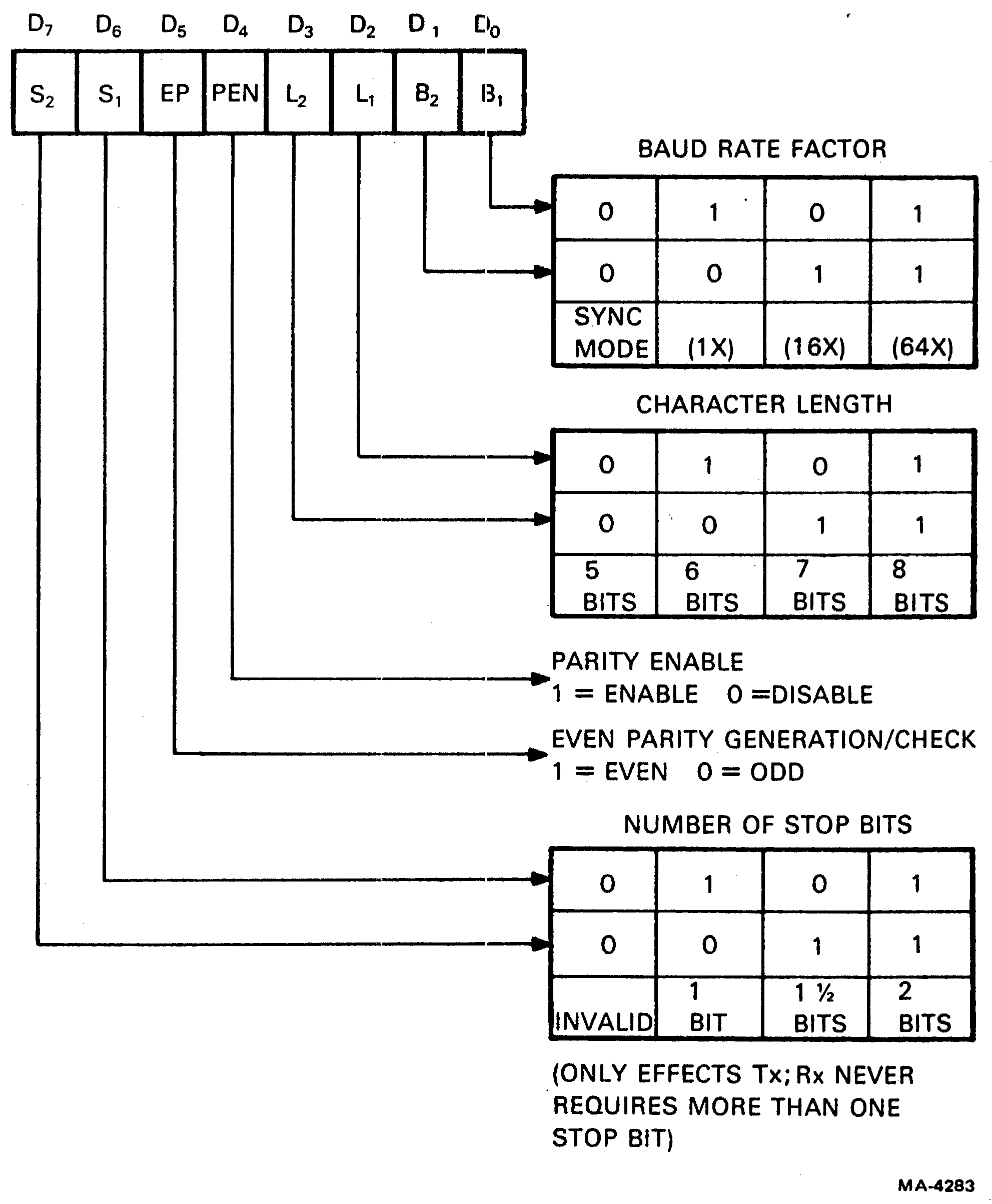
The microprocessor can program the PUSART to operate with several standards and parameters. Many of these parameters are predetermined by the VT100 specifications. Character length, number of stop bits, parity enabling and format, baud rate multiplication factor, and asynchronous operation are all programmed in at power-up through the mode instruction (Figure 4-3-3) from the stored SET-UP information. Address bit A00 selects either the command register in the PUSART for writing the byte containing this information, or the transmit buffer for normal operation. A different programmable device, discussed later, provides the selected baud rate from SET-UP data.
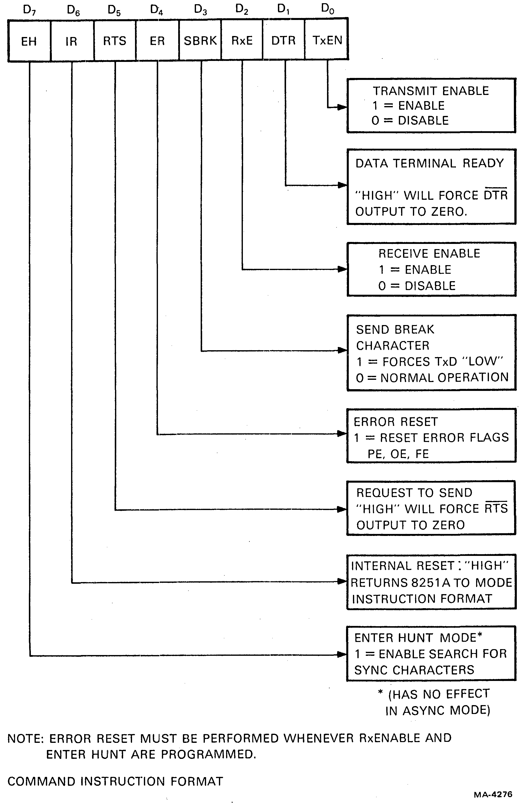
After the PUSART mode of operation is selected by writing a mode instruction, PUSART operation is controlled by writing a command instruction (Figure 4-3-4). Once the mode instruction has been written into the PUSART, all further “control writes” (C/D̅=1) load a command instruction. A reset operation (internal or external) returns the PUSART to the mode instruction format.
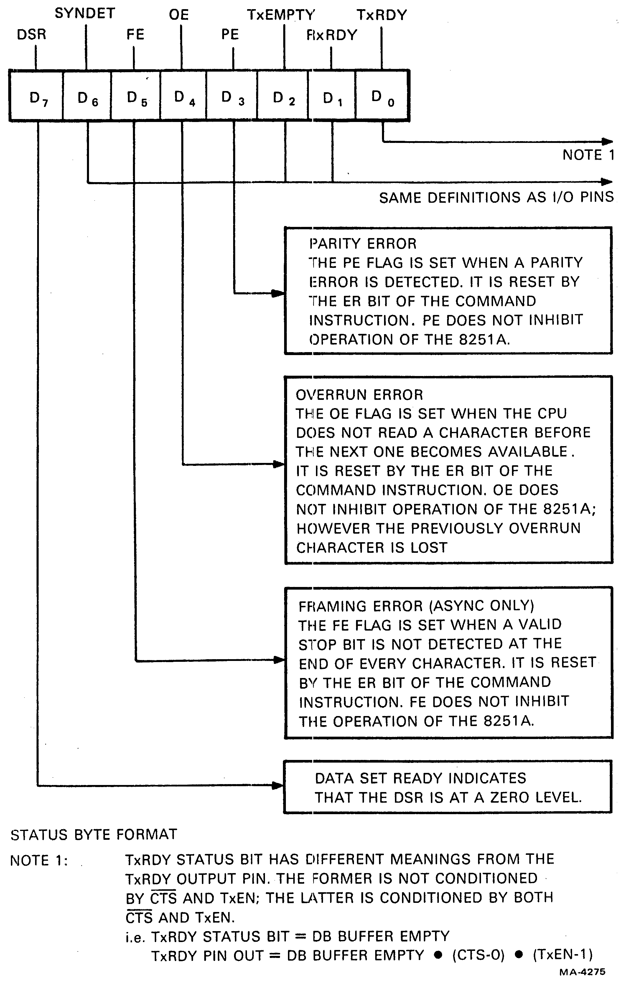
The status of the PUSART can be read by the microprocessor by performing a read with C/D̅=1. Some of the bits in the status word (Figure 4-3-5) have the same meaning as output pins on the PUSART chip. The status word may be a maximum of 28 clock periods behind the event causing the update. This clock, from the microprocessor’s phase 2 TTL signal, is the clock for the internal operation of the PUSART, which is a dynamic device requiring internal refresh at regular intervals.
When the microprocessor wants to send a character out, it checks the XMIT flag at the flag buffer. If this flag is high the transmit buffer is empty and can accept data. If the flag is low, the microprocessor continues through its background program and returns to check again later.
When the flag is high, the microprocessor loads a data byte into the transmit buffer. The PUSART is double-buffered; this means that there is a second data buffer inside that is automatically loaded from the first buffer. The second buffer’s contents get start and stop bits and parity (if enabled) appended and are shifted out by the continuously running clock. Immediately after the second buffer is loaded, the transmit flag goes high and the first (transmit) buffer can be loaded again.
Any data that appears on the receive data line is shifted into the internal receive shifting buffer. When a full character of bits has arrived, the start, stop, and parity bits are stripped. Parity is checked, and if bad, the parity error flag in the status word is set. Data is transferred to the receive data buffer, and the receive flag is set. This flag requests an interrupt from the microprocessor. The microprocessor then has the amount of time it takes the next character to shift in to read the first character. After reading the character, the microprocessor reads the status byte to check the integrity of the data. If the microprocessor does not read the receive data buffer in time, the second character writes over the first one which is lost. Then, an overrun error is reported in the status word. The checkerboard character appears for all errors.
PUSART clocks are derived from the microprocessor clock. The microprocessor clock crystal was selected to provide a frequency within the limits of the 8080 which could be readily divided to provide standard baud rates. The division occurs in programmable baud rate generator E60. This device contains two independent counters to allow different receive and transmit (split) baud rates. Each counter has 4 input lines to select 1 of 16 rates. Thus, a 1-byte load into the device can set up both send and receive rates. The baud rate generator’s input register is written into as a device in the I/O address space.
E60 is factory mask-programmed with the division ratios required to get standard baud rates from the crystal frequency. The 4-bit input is an address for a ROM location containing the SET-UP information for each rate. Table 4-3-1 lists the baud rate generator divisors.
E60 was originally designed to operate with a crystal as a self-contained crystal controlled oscillator and divider. The oscillator is located elsewhere, so the oscillator inputs EXT1 and EXT2 receive the microprocessor clock driven out of phase by two inverters in E38.
| (Input frequency = 2.76480 MHz) | |||
|---|---|---|---|
| X16 Baud Rate | Divisor | Output | Freq (Hz) Error |
| 50 | 3456 | 800 | |
| 75 | 2304 | 1200 | |
| 110 | 1571 | 1760* | -0.006% |
| 134.5 | 1285 | 2152* | -0.019% |
| 150 | 1152 | 2400 | |
| 200 | 864 | 3200 | |
| 300 | 576 | 4000 | |
| 600 | 288 | 9600 | |
| 1200 | 144 | 19200 | |
| 1800 | 96 | 28800 | |
| 2000 | 86 | 32000* | +0.465% |
| 2400 | 72 | 38400 | |
| 3600 | 48 | 57600 | |
| 4800 | 36 | 76800 | |
| 9600 | 18 | 153600 | |
| 1900 | 9 | 307200 | |
| * Output frequency shown is nominal value. Include percentage error to get actual frequency. | |||
The serial transmit and receive interfaces are ICs that convert between TTL signals and EIA RS-232-C unbalanced bipolar signals. The electrical specifications and connector pinouts are described in Chapter 3, Installation.
Certain pins on the PUSART are labeled with standard modem control designations. These pins are readable [Data Set Ready (DSR)] or writable [Data Terminal Ready (DTR)] and [Request to Send (RTS)] as buffered bits in the PUSART’s status and control bytes. Other signals from the modem pass through EIA level translators with Schmitt trigger inputs to a tristate buffer which, when enabled by the MODEM RD command, presents them to the data bus. Another signal [Speed Select (SPDS)] is written from the data bus into the NVR latch which is a convenient extra latch position. None of these signals are used to support modem control in the basic VT100. They are always programmed at power-up to allow normal full duplex operation with some modems when a standard EIA cable is installed between the modem and the VT100. See Chapter 3 for more interface information.
Three kinds of data can be exchanged between the VT100 and the host: control characters, control functions, and displayable characters.
Control characters are any ASCII characters in the range 0 - 1FH. They include carriage return and line feed.
Control functions start with a control character (escape) and contain additional characters which extend the range of special actions that the terminal can perform. Cursor home is such an action. Some control functions can contain numeric parameters to modify the special actions. Direct cursor addressing is a typical example. Appendix A of this manual describes the programming and use of the control characters and functions in detail.
Displayable characters are those ASCII codes that are stored in the screen RAM, causing a character to be displayed on the screen.
The microprocessor checks each character as it comes in from the PUSART. Only four characters cause any special action at this time. Control codes XON and XOFF (see below) are immediately processed while NULL and DELETE are discarded. Everything else gets put in a 64 character (128 characters in later model terminals) first-in/first-out space in the scratch area of RAM called the SILO. The SILO processor routine maintains this area by updating two locations called SILIN and SILOUT. These point to the current entry and exit points in a loop of memory locations. The farther apart they are, the more characters are in the SILO. The addresses of the two points are subtracted from each other to determine the filling of the SILO. The subtraction is performed in modulo 64 (or 128) arithmetic to accommodate the rotation of the locations.
The SILO is necessary because when the microprocessor reads a character, it acts on that character completely before taking another one. For example, a line feed character causes the processing needed to accomplish a scroll. The processing time often exceeds the time between characters at the port. To save the characters that might arrive and get lost during a special action, the microprocessor responds to the received data interrupt by quickly moving the data to the SILO. Only the examination described above gets performed. After the current action is finished, the microprocessor gets the longest waiting character out of the SILO and range checks it. If it is less than 20H, it is a control character and the microprocessor processes it. If it is 20H or above, the microprocessor puts it in the next character position in the screen RAM.
XON and XOFF are two control codes that the terminal and host may send to each other to control the pace of data transmission. The host usually has a buffer space similar in function to the VT100’s SILO. If either device has a large processing load at the same time that a lot of data is being received, the buffer or SILO can fill up. The receiving device monitors its buffer and sends Transmit Off (XOFF) when the buffer contains a predetermined number of characters. On the VT100 this value is 32 characters. (A second XOFF is sent at 112 characters in late model VT100s.) The sending device should stop transmitting until it receives Transmit On (XON). When the receiving device empties its buffer to another predetermined number of characters (16 characters on the VT100), it sends XON.
The NO SCROLL key on the keyboard enables and disables SILO fetching. If data continues to arrive, the SILO management routine sends XOFF or XON as required. The microprocessor keeps track of the current state and sends the opposite command the next time the key is pressed. CTRL-S and CTRL-Q send XOFF and XON directly. Coordination of various causes of XON and XOFF is discussed in Appendix A.
Because of the serial interface, several character times may elapse before the transmitter acts on XOFF and its last character passes through the receiver. This partly determines how full the buffer can be before XOFF must be sent. The other determinant is the worst case condition in split speed operation. If the terminal transmits at a low speed and receives at a high speed, the interface delay can allow several characters to arrive before XOFF stops their transmission. A detailed discussion of this problem is in Appendix A.
A parser is a routine that examines a sequence of characters. It then starts processes and extracts parameters based on the contents of the sequence. The term comes from the grammarian’s practice of parsing (separating) a sentence into its component parts: subject, verb, object. The meanings of many sequences are being standardized throughout the data processing industry through American Standards Institute (ANSI) and International Organization of Standardization (ISO) committees. The VT100 employs a subset of several of these standards, plus it has several private sequences to allow it to perform certain DEC-specific functions like behaving as a VT52.
A character in the range below 20H is always the starting flag for the parsing process. Some functions have only the first character for their sequence; line feed (0AH) is an example. After the function is performed, the next character is taken from the SILO. If it is not in the control range, it is put on the screen. Escape (1BH) is the flag for a longer sequence. After escape, characters are taken from the SILO and range-checked as intermediate (20H to 2FH) or final (30H to 7EH) until a final character appears. The sequence is interpreted and the appropriate function performed. Then the next character is taken from the SILO and displayed if not in the control range. If a sequence is not supported by the VT100, it is parsed and then ignored.
Detailed descriptions of the functions are in the VT100 User Guide and in Appendix A of this manual.
In local mode, keyboard output bypasses the communication transmitter and receiver and SILO and is acted on directly. The Data Terminal Ready signal (DTR) at the EIA interface is unasserted in local.
The standard terminal port (STP) is a printed circuit board edge connector on the basic video board that contains twenty pairs of contacts. When no board is plugged into the connector, the pairs of contacts meet. All EIA data and modem control signals plus the two baud clocks pass through this connector. Future options may utilize the signals present at this connector. For a complete discussion of the details of the STP, see the STP Option Interface Guide, Chapter 7.
The VT100 can test its communication circuits, but because the operator must temporarily plug in a specially wired loopback connector, the test is not performed automatically. Refer to the Service chapter for instructions. There are two tests. One is a data test for either 20 mA current loop or EIA interfaces. This test transmits a pattern of data out the transmit line and examines the data as it returns through the receive line. Each bit of the data bus is tested with the eight test characters: 01H, 02H, 04H, 08H, 10H, 20H, 40H, 80H. This group of eight passes through the circuit repeatedly while the microprocessor changes the baud rate after each pass.
The second test, for EIA only, tests the modem control lines to ensure that they can be controlled. Some terminal controller modules have an etch revision at E39 that does not permit EIA testing. These modules can be recognized by the presence of extra wires attached at E39.
Table 4-3-2 lists the test connector wiring.
| From | To | |
|---|---|---|
| EIA: | Pin 2 | Pins 3 and 15 |
| Pin4 | Pins 5 and 8 | |
| Pin 20 | Pins 6 and 22 | |
| Pin 19 | Pins 12 and 17 | |
| 20mA: | Pin 1 | Pin 3 |
| Pin 2 | Pin 7 | |
| Pin 5 | Pin 8 |
The VT100 keyboard is a typewriter-like array of momentary, normally-open switches. The array is mounted in a small case with a speaker for audio feedback and electronics for interfacing the array to the terminal. The VT100 keyboard connects to the terminal controller board through a three conductor cable that plugs into the back of the terminal cabinet. The cable carries power, ground, and a complex bidirectional data and clock signal. The terminal sends the clock signal and a status word that controls the LED indicators, the bell, and the keyboard scan process. The keyboard sends the row and column address of each key that is pressed. The terminal’s microprocessor then translates that address into an ASCII character and transmits it serially to the host through a UART or performs internal actions such as SET-UP and no-scroll. Refer to Section 4.3 for a discussion of UART principles.
This section describes the operation of the keyboard and its interface hardware and software in the terminal.
The bidirectional interface separates incoming from outgoing data on the single signal line. Incoming data from the terminal contains a clock that passes directly to the UART and the address counter circuit. Then the data and clock are integrated. The duty cycle encoded data becomes serial data. The UART deserializes the terminal data and produces an 8-bit parallel output. These bits control the bell and LEDs, and start address scanning, depending on which bits were set by the terminal in the keyboard status byte.
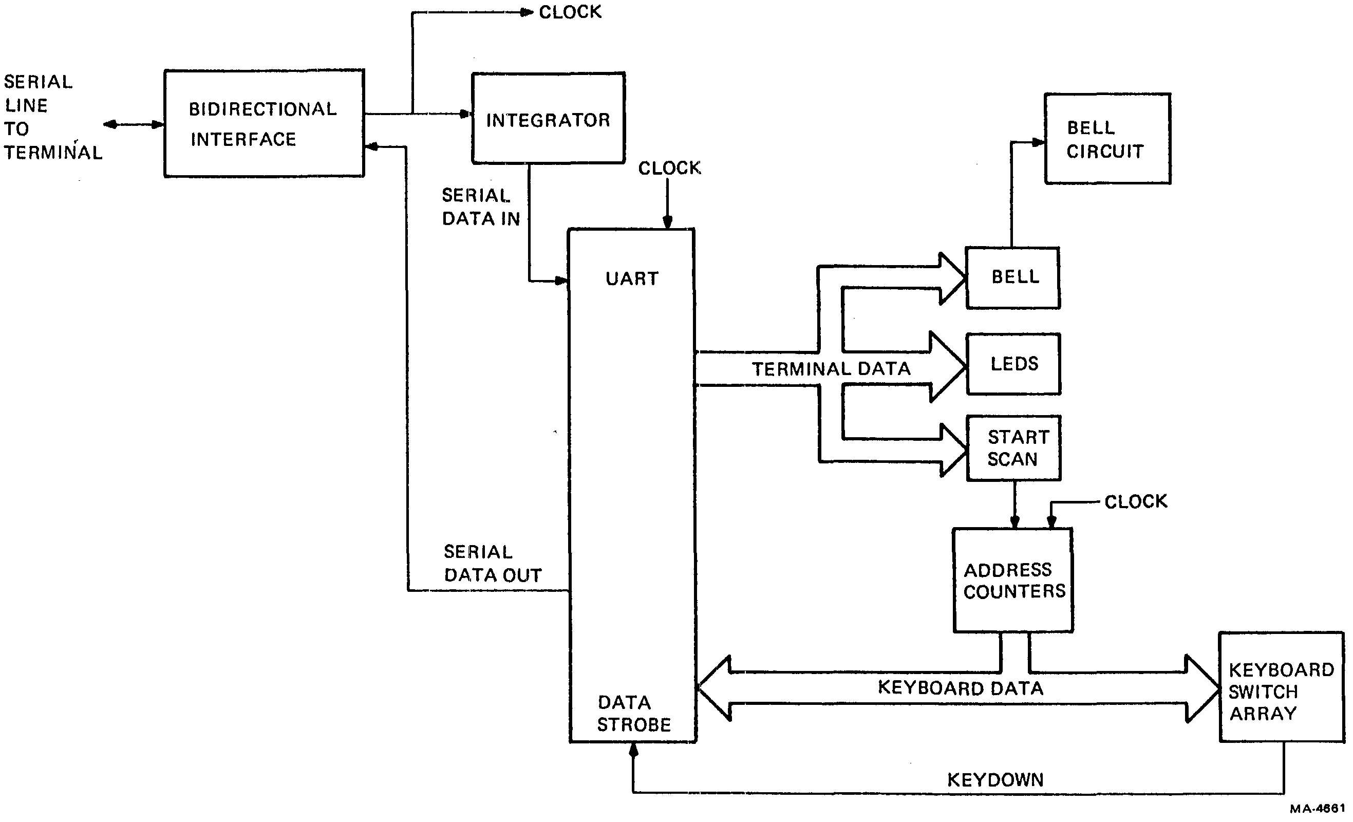
The address counters start on command and send row and column addresses to the keyboard switch array. When an address matches a key that is down, the Key Down signal strobes that address into the UART. The UART serializes the address and the bidirectional interface sends it to the terminal.
Information is exchanged between the terminal and the keyboard in serial form. One start bit, eight data bits, and one stop bit are transmitted using a clock derived from the horizontal timing circuits in the terminal. Besides timing the serialization of data in the terminal, the clock is also transmitted to the keyboard to time its circuits. The terminal data is a status byte that controls the keyboard by commanding key scans and other functions.
The keyboard transmits its data in the same format and with the same clock. Its data are the addresses of whatever keys are down during a scan. The last key address sent has the highest address possible and is always sent to indicate to the microprocessor that the scan is complete.
The terminal controls the keyboard through a status byte that it sends through the interface along with the keyboard clock. The first six bits of the 8-bit byte (Figure 4-4-2) control the On-Line/Local, Keyboard Locked, and four user programmable LEDs on the keyboard. Every time the status byte is sent, it refreshes the LEDs even if no new action is being taken. The seventh bit is sent only once in a vertical interval and initiates the scanning process in the keyboard. The eighth bit, if sent only once, causes the keyboard speaker to click. (Keyclick is defeatable at SET-UP.) If the bit is sent approximately two hundred times in a row, for about a quarter second, it sounds a bell.
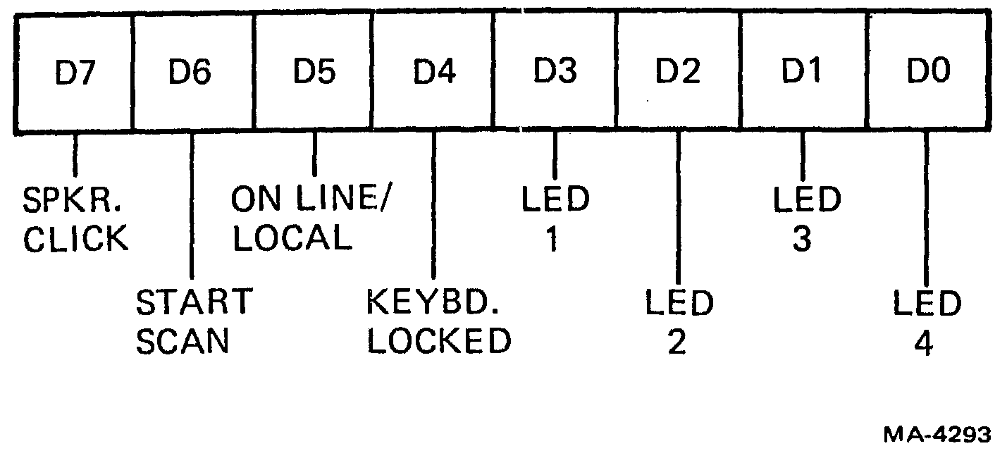
The operating clock for the keyboard interface comes from an address line in the video processor (LBA4). This signal has an average period of 7.945 microseconds. Each data byte is transmitted with one start bit and one stop bit, and each bit lasts 16 clock periods. The total time for each data byte is 160 times 7.945 or 1.27 milliseconds. Each time the Transmit Buffer Empty flag on the terminal’s UART gets set (when the current byte is being transmitted), the microprocessor loads another byte into the transmit buffer. In this way, the stream of status bytes to the keyboard is continuous.
Keyboard addresses are outputs from a counter that correspond to locations in a keyswitch matrix. The counter can address all locations in the matrix. If a keyswitch is closed, the counter output addressing that location is transmitted. The address counter is a pair of 4-bit binary counters arranged so that only the top seven bits go to the switch matrix. These outputs also connect directly to the UART transmit data inputs. The output of the first bit in the counter is a squarewave with a period equal to the amount of time that each key is sampled during a scan. Key Down L appears at the input to flip-flop E6 when the counter reaches the address of a key that is pressed. Half a sample period later, the first counter bit clocks the Key Down signal through flip-flop E6. The half period delay allows any glitches in the address counter to settle before Key Down asserts Data Strobe. Data Strobe loads the UART transmit buffer with the address count present at the data input at that moment. That address count represents the key that was down when Key Down was asserted.
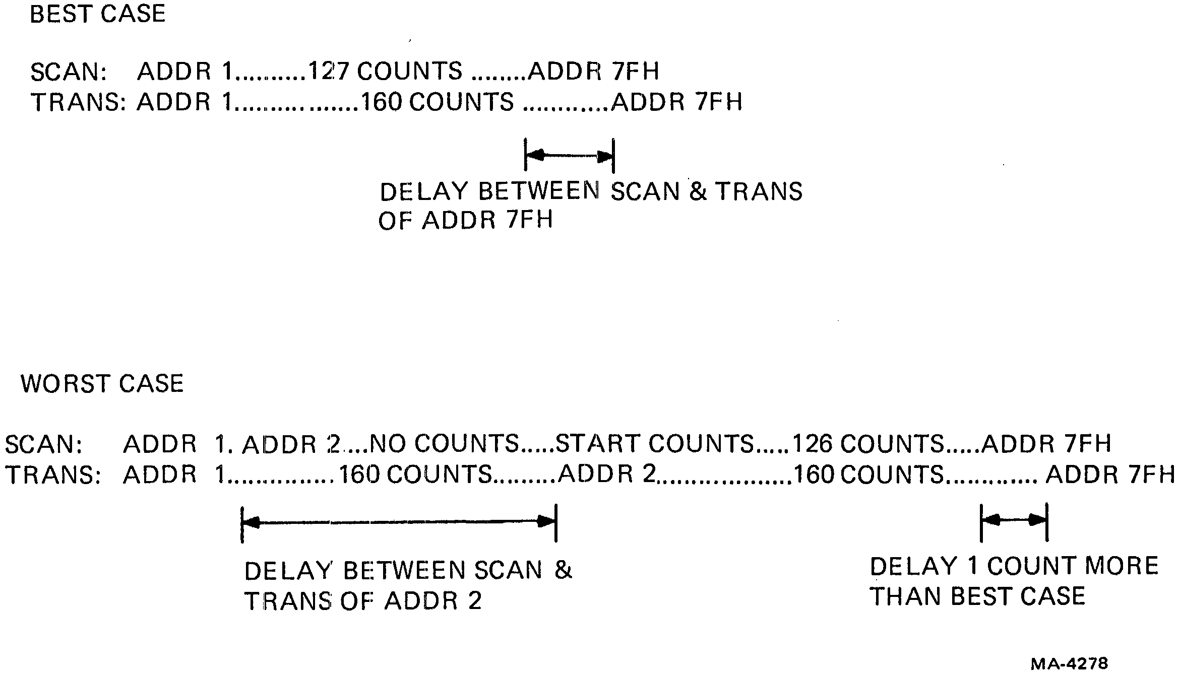
The UART, which is double-buffered, deasserts Transmit Buffer Empty while the transmit (outer) buffer is full. This stops the counter by blocking the clock at gate E4. As soon as the data moves into the inner shifting register, the transmit buffer empties, TBMT is asserted, and the count continues. In this way, any number of key addresses can be sent to the terminal. The time the scan takes to finish varies with the number of keys down. On the first address load, when transfer from the transmit buffer into the shifting register is immediate, the UART reasserts TBMT almost immediately. For loads later in the scan, the UART deasserts TBMT for a longer period because an address that loads into the transmit buffer must wait with the counter stopped until the previous transmission is done. Because the transmission time is 160 counts and the complete address scan takes only 128 counts, there is a minimum wait of 32 counts or about 20 percent of a character transmission time between the scan of address 7FH and the transmission of address 7FH if the first key in the scan was down. (Refer to Figure 4-4-3.)
Because it is hard-wired, the highest address (7FH) always asserts Key Down and gets transmitted, indicating end of scan to the terminal. The highest bit also clocks flip-flop E3 which clears the counters and stops the count. This is the only way that the scan is terminated. The scan begins again when the terminal sends the Start Scan bit in the status byte to the keyboard. When the data arrives, the UART asserts its Data Available flag. On the next clock transition, flip-flop E6 passes a short, clock-synchronized Data Available pulse to gate E5, resetting the flag in the process. E5 combines the Data Available pulse with the Start Scan bit if present to clear E3, allowing the count to begin.
After the terminal starts the scan, it waits for the 7FH address and then for a vertical interrupt (a synchronizing signal explained in VIDEO) before it will start the scan again. If there are a lot of keys down, the scan may take more than one vertical interval to finish. The keyboard ignores further requests to scan until the current scan is complete.
Here is a formula that estimates the delay between the time that the terminal asserts the start scan bit at its UART and the time that the terminal UART asserts data available upon receiving the final address 7FH. The clock driving the address counter and UART has a period of 7.945 microseconds, there is the number of addresses to the first closed key to be counted, and the serial transmission of an address takes 160 clock periods (16 clocks per bit, 8 data bits, 1 start and 1 stop bit).
| 160 | start scan command word to keyboard | ||
| + | m | counts to first key | |
| + | n × | 160 | for n keys down |
| + | 160 | transmission of 7FH | |
| Total × 7.945 = microseconds | |||
For example, suppose that one key, #24, is down.
| 160 | start scan command word to keyboard | ||
| + | 24 | counts | |
| + | 160 | transmission of key #24 address | |
| + | 160 | transmission of 7FH | |
| 504 × 7.945 = 4004 microseconds (4.0 µs) [TYPO?] | |||
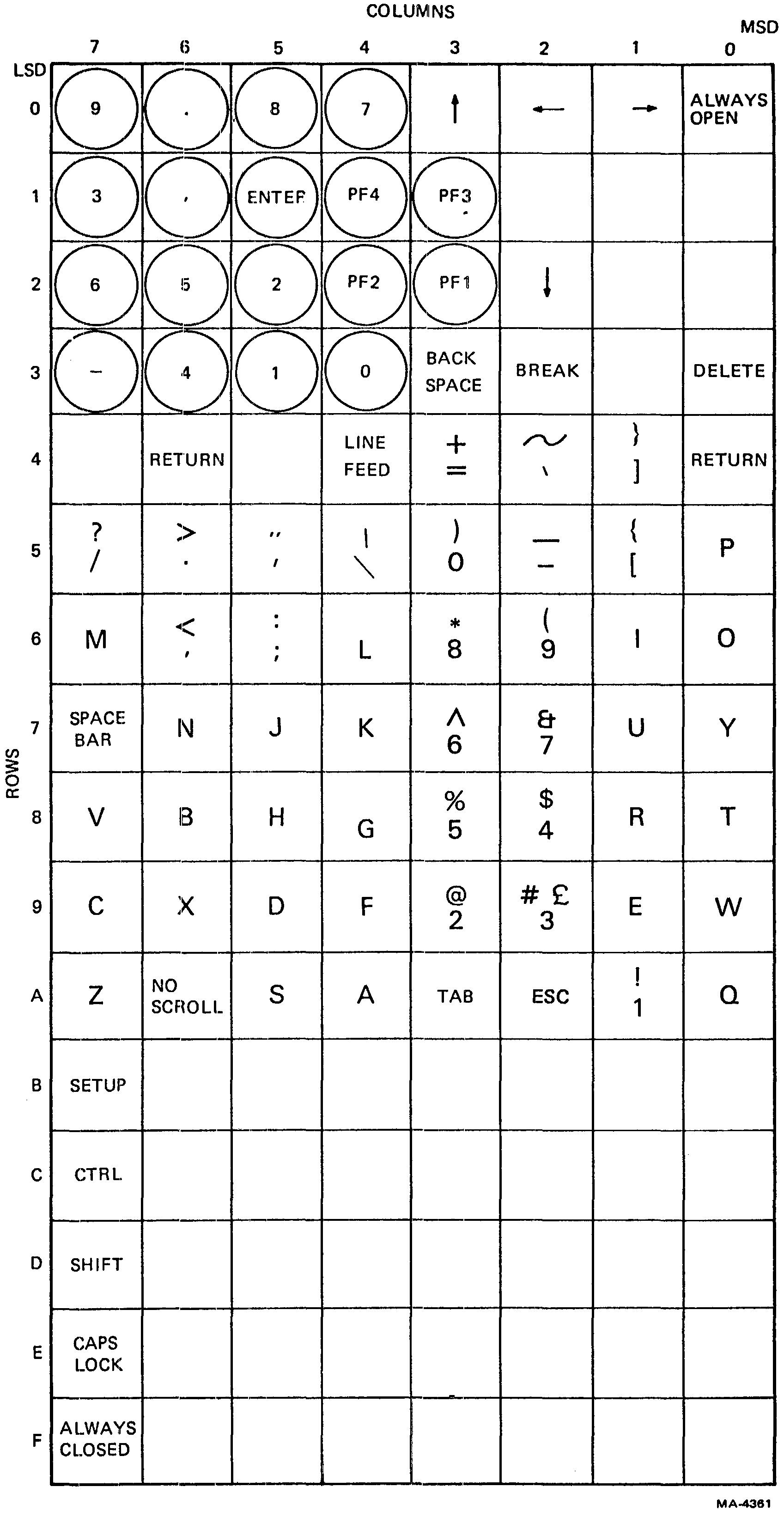
The keyboard is an array of contact pairs arranged in 16 rows and 8 columns (Figure 4-4-4). One side of each pair is connected to all the others in its column and each column connects to +5 volts through a resistor. Each of the eight columns also connects to an input on the eight-to-one multiplexer E14. The other side of each contact pair connects to all the others in its row and to an output on one of the one-to-eight demultiplexers E11 and E13. The seven outputs of the keyboard scan counter control the multiplexer and demultiplexers. The rows are selected by the lower four bits and the columns by the upper three.
A low input to the selected column line on the multiplexer causes a Key Down L signal. If a key is pressed when the row and column address is not on its position, the unselected demultiplexer line is high and there is no change in level across the contacts. If the demultiplexer line is selected, it is low, and the closed contact pulls the column low through the resistor. Each column is scanned top to bottom as the low four address lines count; then the next column is selected and scanned. The complete keyboard scan takes about 1 millisecond when no keys are down.
The last row and column position (address 7FH) is wired to always indicate key down. This value indicates to the terminal that the scan is ended.
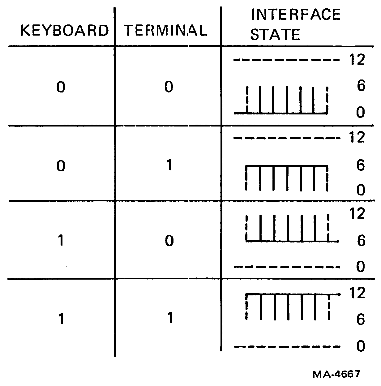
The terminal sends data and clock to the keyboard; the keyboard sends data only. Transmission is asynchronous, full duplex, serial, 8-bit data with one start bit and one stop bit over a single signal line. Four states can exist on the line, representing the two signal states from each end of the line.
Both signals may coexist on the same wire, originate at opposite ends, and simultaneously communicate provided that sensing resistors are put at each end. The interface works by observing the voltage variations on its input (across the sensing resistor) while biasing the input in an opposite direction with its own output signals so that only input variations can cause enough change to exceed the threshold of detection.
Refer to the keyboard interface schematic, Figure 4-4-5a. If one side of the line is at +12 volts and the other is at ground, then by Ohm’s Law, the center of the two equal resistors will be at V/2 = 6 volts. If both sides are at 0 or 12, the center will be identically at 0 or 12. Thus the signal line can either have no current flow but with the junction of the two resistors at either 0 or 12 volts, or the junction can be at 6 volts with current flow to the left or to the right, thereby representing the four required states.
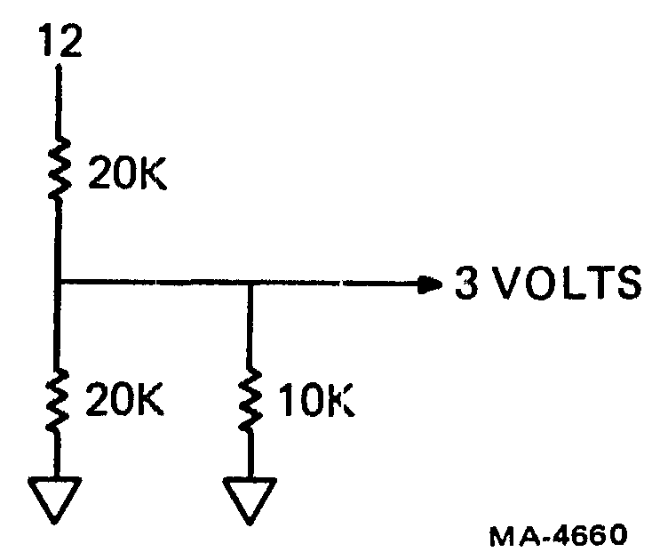
The receiving side of the keyboard interface separates the incoming signal from its own output by delivering a sample of its output to the inverting input of a comparator. Refer back to Figure 4-4-5. This provides an additional input for the comparator which compensates for the variation that occurs on the noninverting input at the same time that the output changes. R12 and R13 (both approximately 20K) and R11 (10K) are a divider providing bias to the comparator. If E8 (an open collector driver) is off (high), then the end of R11 connected to E8 is essentially at +12 volts through R15 (470). The R11, R12, R13 divider outputs 9 volts as shown in Figure 4-4-5b. If E8 is on (low), the end of R11 is at ground, and the divider outputs 3 volts (Figure 4-4-5c).
Meanwhile, the signal from the other end of the signal line is admitted to the noninverting input of the comparator through a resistor (R7) whose value is small compared to the comparator’s high input impedance. The positive feedback resistor R8 provides a small amount of hysteresis to improve the circuit’s noise immunity.
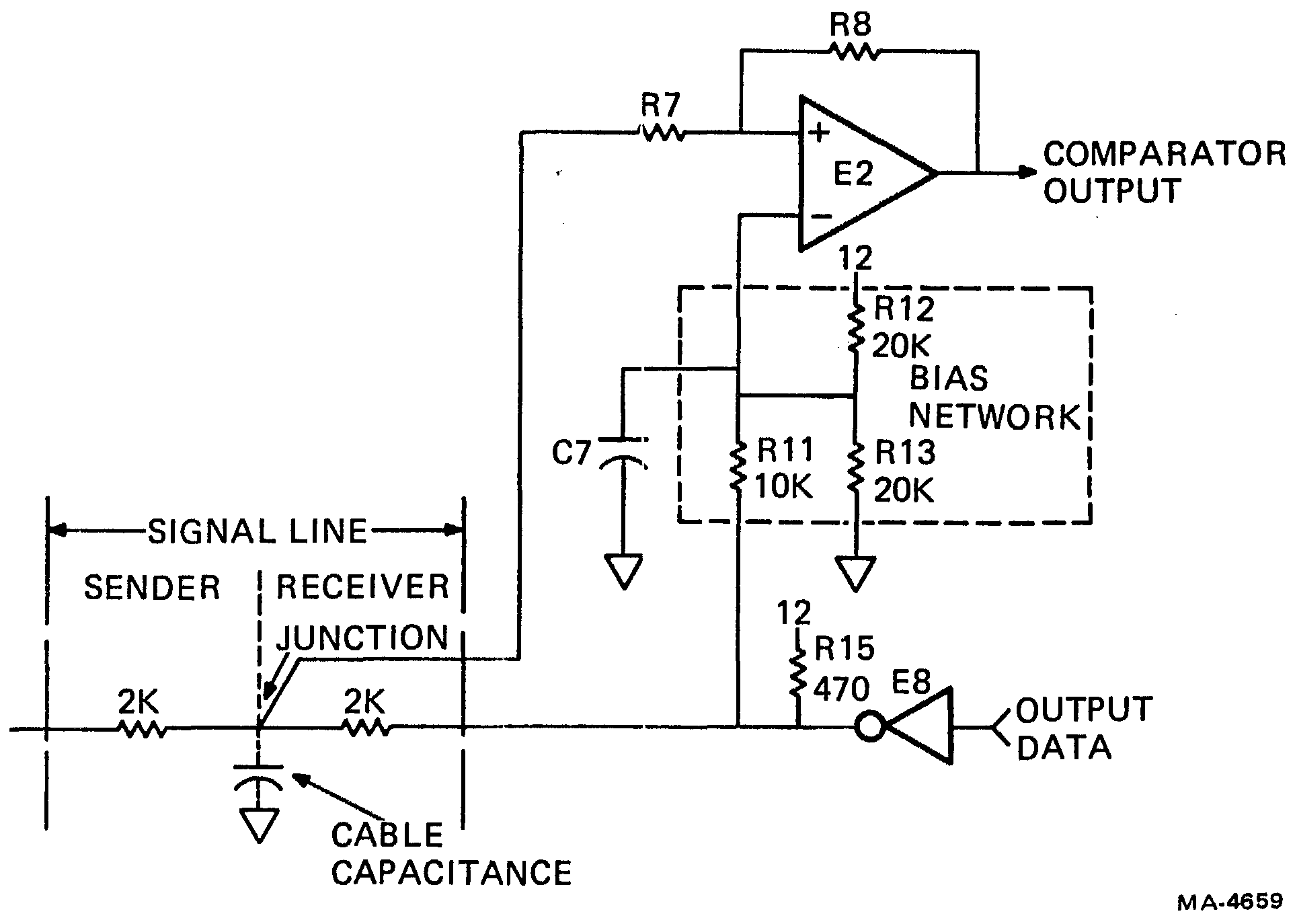
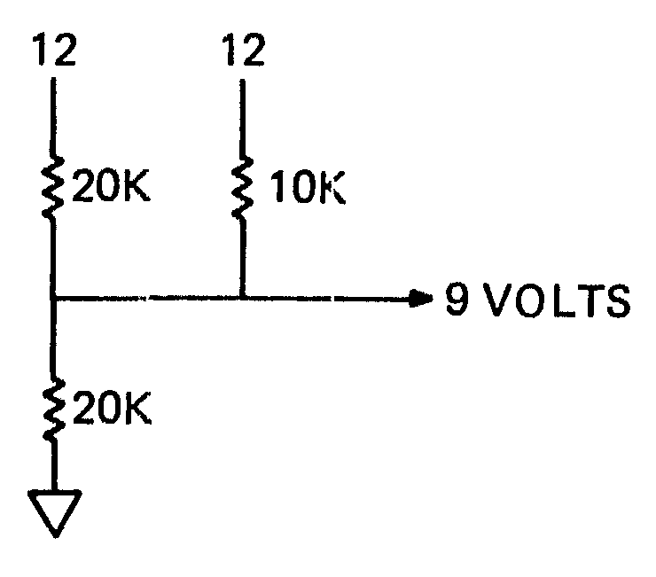
For the case where the junction is at 12 volts, there is no ambiguity about what signal the sender is sending. The comparator must produce a high output because the sender is outputting a high level. (The receiver is also sending a high level but no distinction between the two needs to be made.) The bias network presents a 9 volt signal to the inverting input, so the comparator sees a +3 volt difference and goes high.
For the case where the junction between the sender and the receiver is at 0 volts, there is again no ambiguity. The comparator must produce a low output because both sender and receiver are outputting low levels. The bias network presents a 3 volt signal to the inverting input, so the comparator sees a -3 volt difference and goes low.
For the case where the junction is at 6 volts, either end could be the high or low sender. The decision is made at each end by each circuit examining its own output to decide whether it or the other end is sending a particular level. If the sending end is at 0, the noninverting input sees 6 volts. The receiving end is outputting 12 volts, and the network outputs 9 volts to the inverting input. The comparator sees a difference of -3 volts and outputs low in recognition of the low level at the sending end. If the sending end is at +12, the noninverting input sees 6 volts. The receiving end is outputting 0 volts, and the network outputs 3 volts to the inverting input. The comparator sees a difference of +3 volts and outputs high in recognition of the high level at the sending end.
Table 4-4-1 summarizes the effects of the various signals.
| Send. End | Rec. End | Non-Invert. Input (Junction) | Invert. Input | Difference | Output |
|---|---|---|---|---|---|
| 0 | 0 | 0 | 3 | -3 | 0 |
| 0 | 12 | 6 | 9 | -3 | 0 |
| 12 | 0 | 6 | 3 | +3 | 5 |
| 12 | 12 | 12 | 9 | +3 | 5 |
C7 compensates the circuit for the capacitance of the cable. If C7 were not present, the output of the comparator would glitch when the output driver on the same end of the line changed state. This would be caused by the output signal propagating immediately to the inverting input of the comparator but being delayed (by the RC time constant of the line) to the noninverting input. C7 is chosen so that the time constant of the line is the same at both inputs. Because the resistance seen at the middle of the line is approximately 1000 ohms (two 2K resistors in parallel) and the resistance seen at the inverting input is approximately 5000 ohms (one 10K and two 20K resistors in parallel), C7 is about one-fifth of the cable capacitance. The value is not critical because the ratio of the two time constants can be as large as two and still provide acceptable noise immunity.
The keyboard requires a clock for its operation and is provided with one by the terminal controller side of the interface. To transmit a clock independently of data on the same wire, the terminal side of the interface generates a clock signal within which data is encoded as a pulse width modulation. The terminal circuit produces a 75 percent high pulse width output for the mark state. Data transmission causes the clock output to switch between 75 and 25 percent pulse width (duty cycle).
Figure 4-4-6 is a timing diagram that illustrates the formation of the pulse width modulation. Three nand gates, I, II, and III, combine three signals, Data, LBA 3, and inverted (not) LBA 4. The three gate outputs are wire-ANDed so that all three must have high outputs to produce a high to the out inverter, which drives the terminal’s end of the bidirectional interface. The timing is not precisely correct in this drawing because the LBA signals, addresses to the line buffer in the video processor, are not pure squarewaves and have variations in their periods (see the DC011 section). These variations give the keyboard signal the appearance of clustering in groups of four, but they do not affect the operation of the circuit.
The negative transition of each output pulse occurs at the clock interval regardless of the presence of data. This transition is therefore the reference point for the keyboard clock at the receiving end.
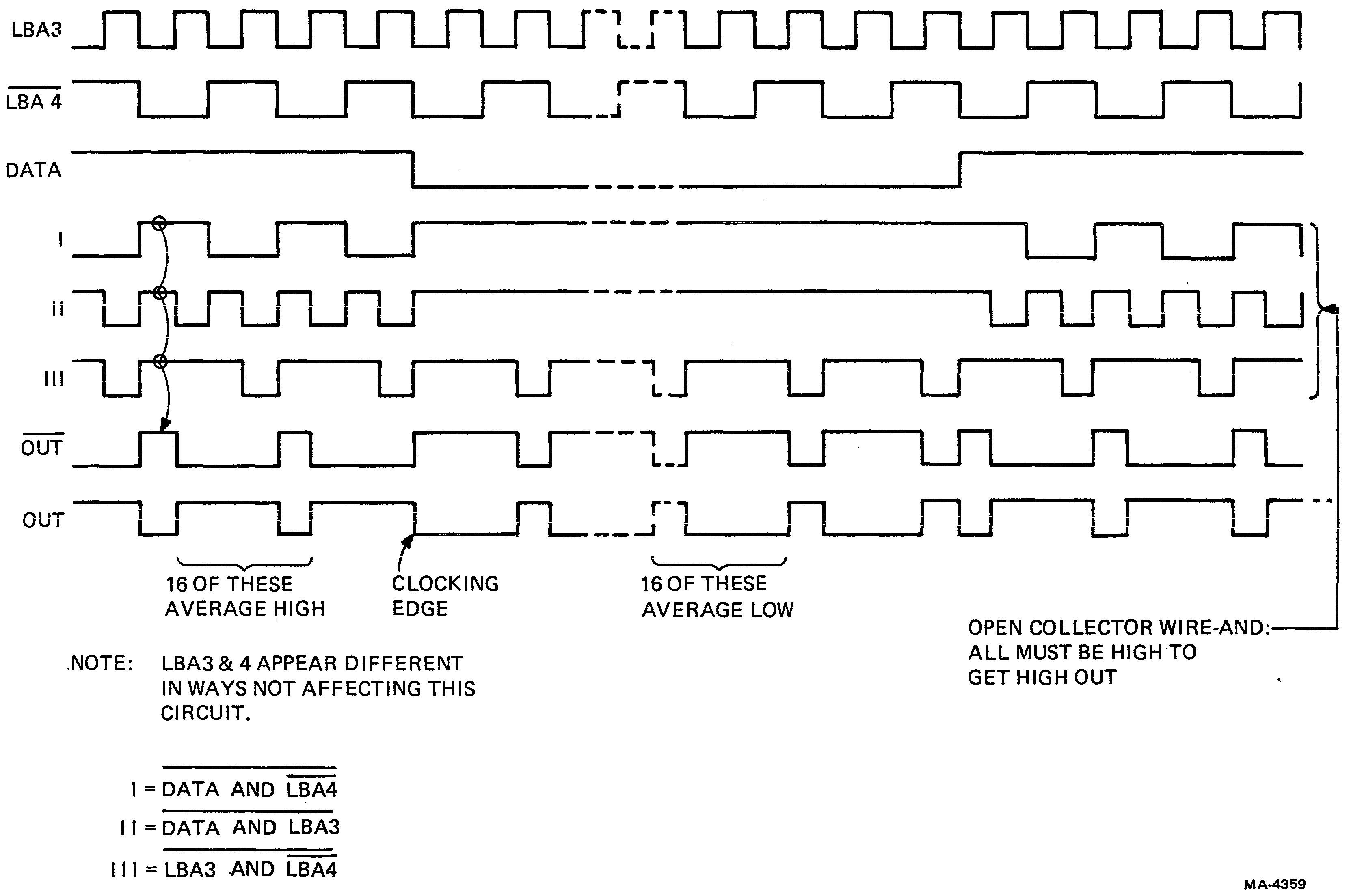
Figure 4-4-7 illustrates the four possible conditions on the interface line when the effect of the clock is included. Figure 4-4-8 shows all four states and the transitions between each of them. Two series sensing resistors in the interface circuit divide the signal in half at the wire. Therefore, although the drivers swing 12 volts at each end, the figures show only 6 volt variations.
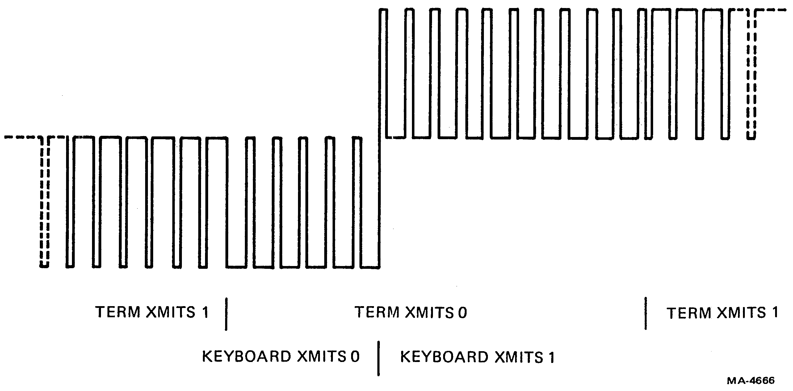
The keyboard recovers the modulated clock signal sent by the terminal but must also separate the data from the clock. The signal is sent directly to the UART and address counter circuits as a clock. The negative edge of the clock occurs at a fixed interval while the positive edge varies according to the duty cycle modulation. The keyboard circuits use the negative edge and ignore the variable pulse width.
Data is extracted from the combined clock-data by a simple resistor-capacitor filter on one input to a comparator. The other comparator input is referred to one-half the power supply. Because the duty cycle of incoming data is either 1/4 or 3/4, the capacitor charges to that proportion of the supply voltage over the 16 clock periods of each bit. The comparator switches when the capacitor voltage rises or falls past the reference value. The short duty cycle of zeros averages to a low voltage that holds the comparator output low. The long duty cycle of ones averages to a high voltage and switches the comparator to a high state. The comparator output goes to the serial data input of the UART where it is deserialized. When all ten bits of a transmitted character are loaded into the UART, it asserts Data Available. This signal enables the bell and scan start if the appropriate bits were set in the byte. The LED bits remain latched at the parallel output of the UART until the next command byte arrives.
The keyboard UART serial output goes directly to an open collector driver that swings its end of the bidirectional signal line between 0 and +12 volts. This is shown as E8 and R15 in Figure 4-4-5a. The circuit is identical at both ends of the interface.
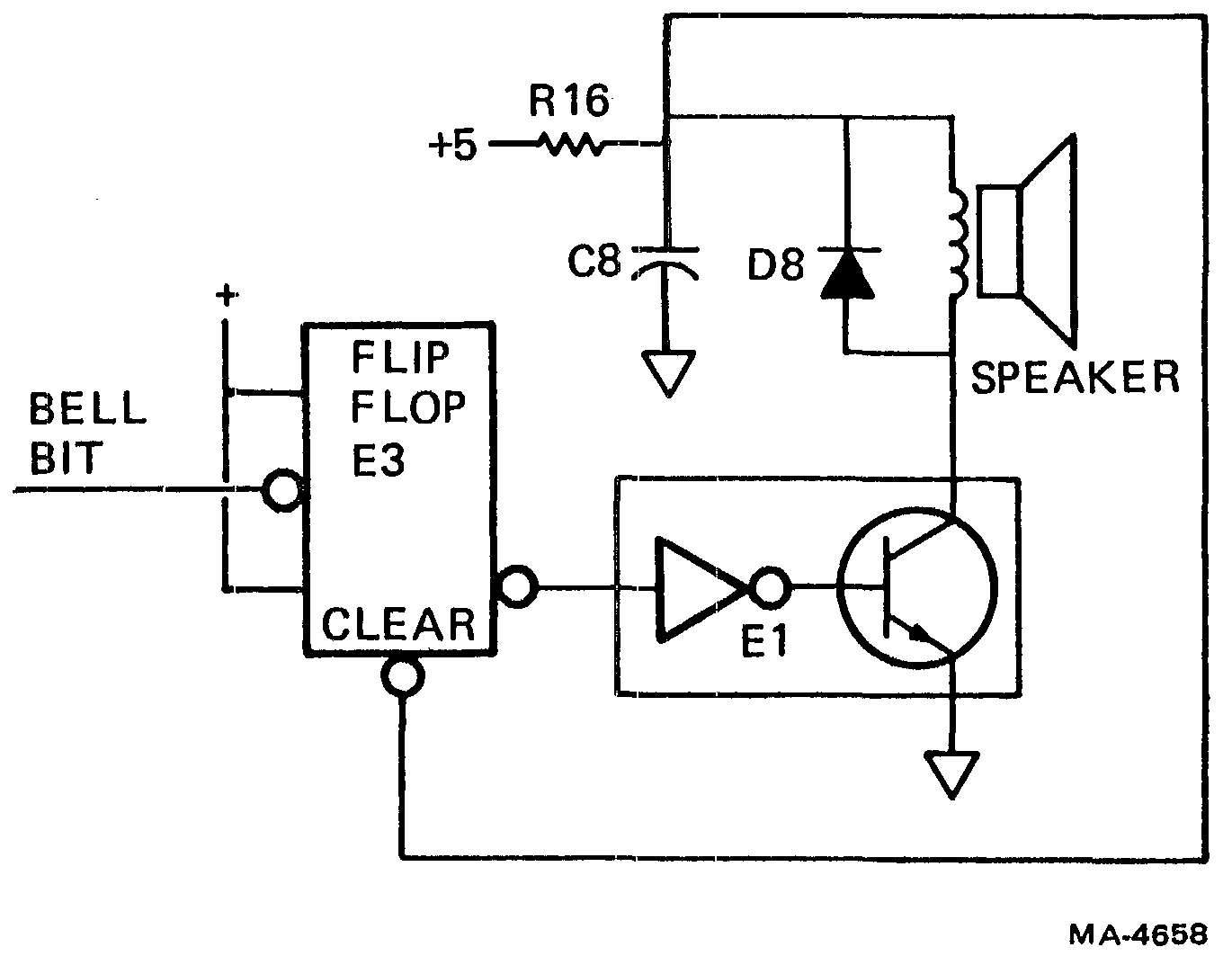
The keyclick/bell circuit provides audio feedback and attention signals for the user. A bit in the keyboard status word controls the bell. Refer to Figure 4-4-9 for the circuit. Capacitor C8 charges to +5 volts through resistor R16. The speaker connects between the capacitor and the collectors of the transistors in E1. When a single status word contains the bell bit, flip-flop E3 toggles and turns on E1. C8 discharges through the speaker and E1, generating a click. When the voltage on C8 falls low enough, it clears E3. E1 turns off and C8 charges up for the next click. The value of C8 is selected to determine the volume of the click. D8 protects the transistors from inductive spikes from the speaker.
If the bell bit is set for many words in succession, the UART latch holds the data output constant. A one clock period pulse from the Data Available flip-flop E6 gates the bell bit through E5 to form a clock to E3. As C8 discharges through the speaker and E1, E3 clears itself, turning E1 off. Then C8 charges up again until the next Data Available pulse clocks E3 on again to repeat the discharge cycle. C8 discharges fast enough so each Data Available pulse (which arrives every 1.28 ms) triggers a cycle, allowing the circuit to produce an 800 hertz tone. Bell is generated by setting the bell bit for 0.25 seconds (about 200 status words). Each cycle of the tone is at a reduced amplitude compared with the single keyclick because R16 is selected to limit C8’s charging rate. The overall effect of the tone burst on the ear is that of a beep.
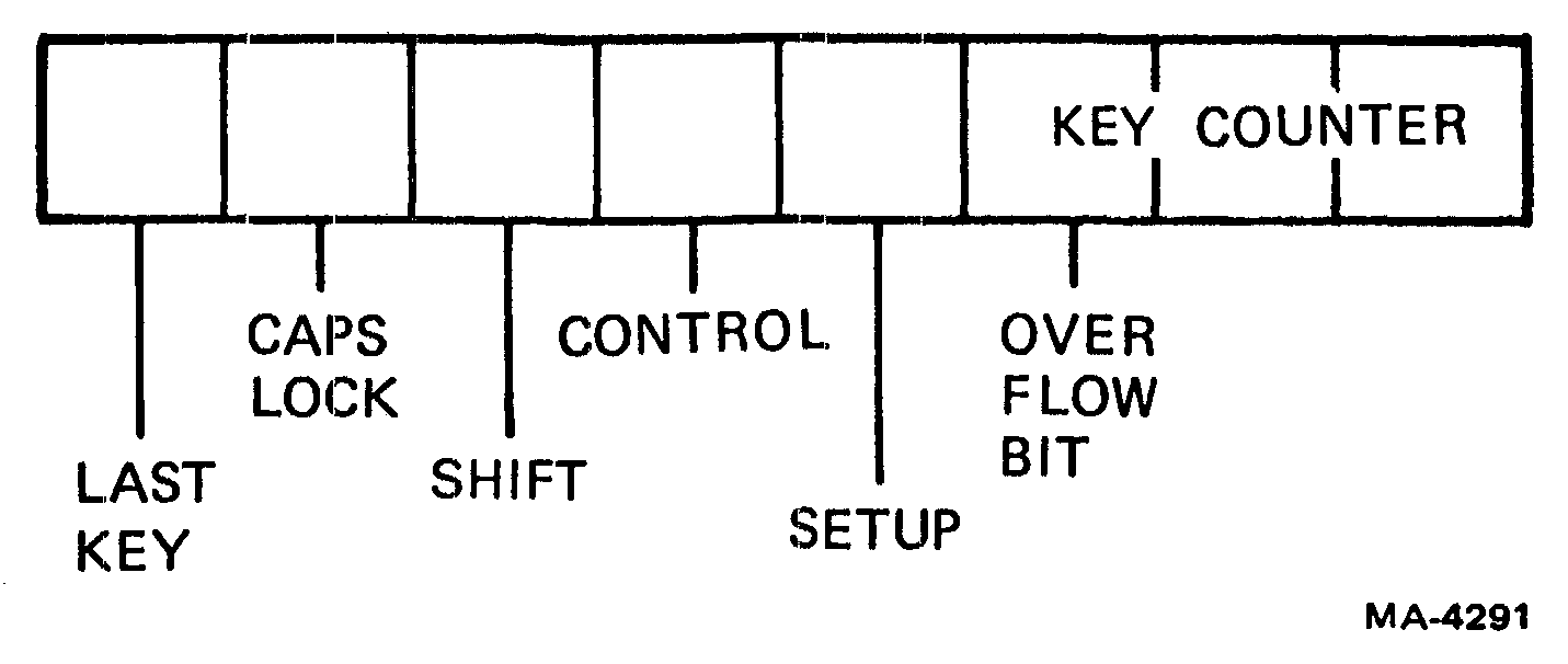
When the microprocessor responds to an interrupt from the keyboard UART and reads a key address from the UART data output, it immediately range tests the address. The function key addresses are all above the regular key addresses, with SET-UP the lowest at 7BH and the always down Last Key at 7FH. An incoming function key address causes a bit to be set in a flag byte called Keys (Figure 4-4-10).
When a key address below the function range arrives, the microprocessor checks the low three bits in Keys for the key count. If the count is less than three, the key address is stored in a three place New Key Address Buffer and the counter is incremented. If the count is already three, the counter is incremented but the key address is discarded.
The logical keyboard processor is that portion of the operating firmware that manages the interpretation and transmission of keyboard data. It consists of several processes.
For a key to be recognized as a new key, it must not have been down in the scan before entry is accepted. The microprocessor checks each key’s history at each scan. If a key was down during the last scan, it is old and is not entered. Only new keys, those not previously seen, are entered. This system allows a key to be held down without being continuously entered at each scan. (This process and auto repeat are discussed later.)
If a key is detected as down for the first time in a while, the microprocessor assumes that it has been pressed. During the scan when the key is first down, the contacts may bounce for several milliseconds. The time window when the contact is scanned is very short. If the contact happens to be bouncing open during that interval, it is not detected in that scan but the time between scans is long so it is finished bouncing by the next scan and is detected normally. If the contact happens to be closed for the first scan while still bouncing, it is detected. It is also detected on the next scan after it has stopped bouncing but now it is an old key and is not reentered.
When the microprocessor is free to perform its background routines, it processes the results of the last keyboard scan. First it checks the high bit of the Key’s byte to see if the scan is finished. If it is not, the microprocessor continues with other work (exits). If it is, the microprocessor checks the key counter overflow bit representing four or more keys sent in the scan. If the bit is set, the microprocessor clears the New Key Address Buffer and exits.
If the overflow bit is not set, the first key is taken from the new key address buffer and tested. If it is either the SET-UP or NO SCROLL key, the microprocessor acts on it immediately and branches to the appropriate routine. It then returns to the keyboard process. (Refer to the microprocessor section for a discussion of SET-UP and to the Communication section for no scroll.)
Another three place buffer contains the keys from the last scan. The microprocessor compares the three new keys with those in the old key buffer. If an old key is not in the new key address buffer, that key is cleared from the old key buffer. New keys then go into the old key buffer. Each key address is only seven bits long, so the high bit in each key entry is used to indicate how long that entry has been in the buffer. If a key is new, the bit is set to 0. This means that the microprocessor has only seen the key once. If the key appears in the new key address buffer on the next scan, the microprocessor sets the high bit to 1, converts the key address to an ASCII code, and sends it to the keycode buffer. Only one key is converted and sent in each cycle of the logical keyboard processor routine. Since the set bit indicates that the key has been sent, in the next cycle that key will be ignored and the next key will be processed.
Key rollover means that more than one key can be down at the same time and be accepted. Normally the VT100 accepts 3-key rollover. If the keys were pressed during different keyboard scans, they will be accepted in the order in which they were pressed. If they were all pressed during the same keyboard scan, they will be accepted in the order of their addresses.
Certain conditions will limit the rollover to only two keys. The 2.5 key rollover specification reflects the presence of these conditions. Because there are no isolating diodes in the switch matrix, certain patterns of contact closure can produce false key down indications. Specifically, three switches closed in three corners of a rectangular pattern, as in Figure 4-4-11, will cause a fourth apparent key address to be sent to the terminal. (Refer back to Figure 4-4-3 to see how the pattern fits into the row-column configuration.) For this reason, although any number of key addresses may be sent by the keyboard during a scan, no more than three may be sent if any are to be accepted. If four or more appear, the terminal ignores all of them and waits for a scan with only three. The special function keys (SHIFT, CAPS LOCK, CONTROL, SET-UP) are in a part of the matrix where there is no pattern sensitivity and no ambiguity. They all are accepted in the same scan with the regular keys and are not counted in the 3-key maximum.
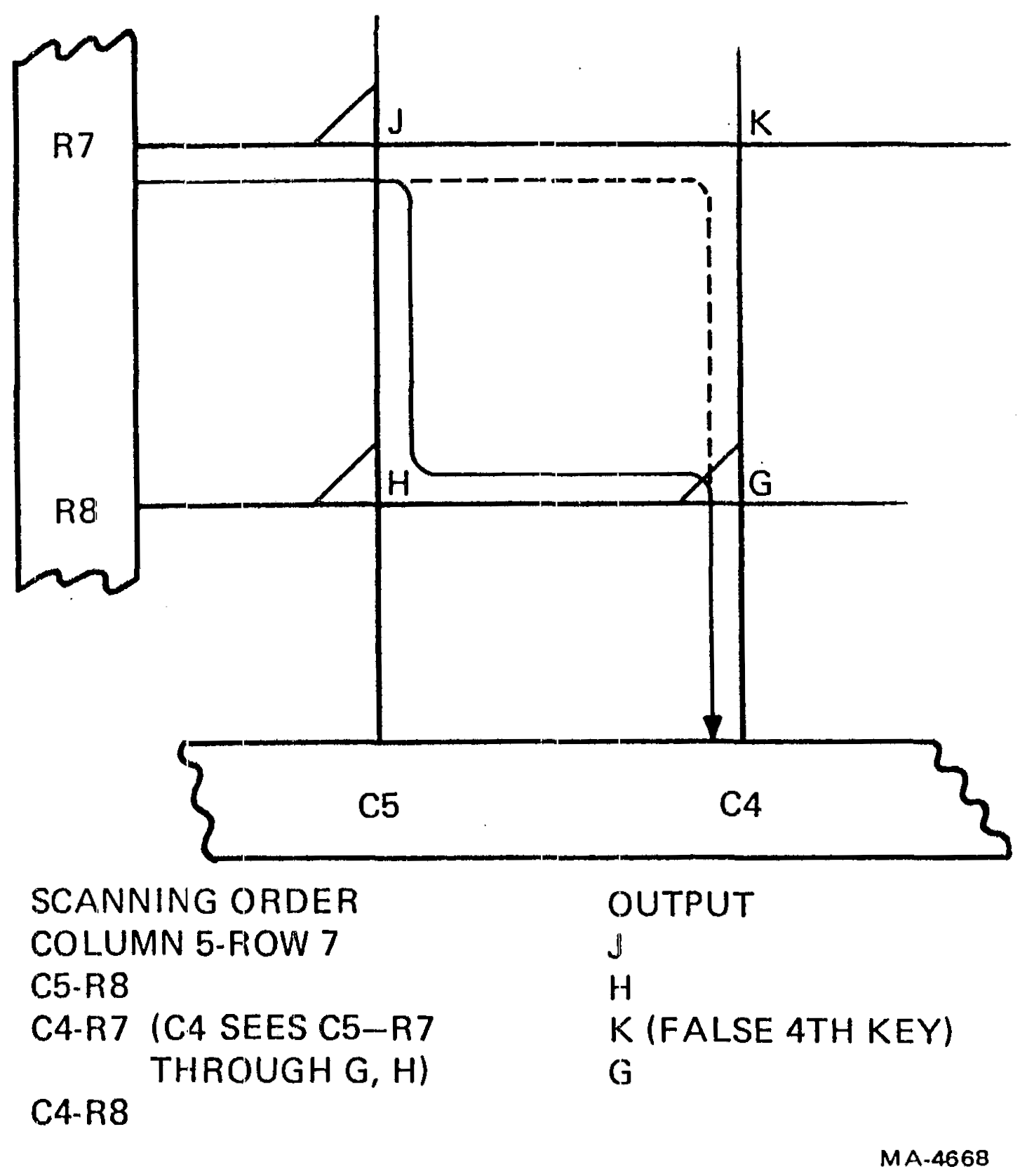
The sneak path problem is also the reason that the keyboard processor looks for the appearance of a key in two successive scans. In Figure 4-4-11, the keys are scanned in the order J, H, K, G. Normally, the keyboard processor counts the number of keys in a scan and ignores all of them if the count is over three, as it is in this case. But it is possible for a user to briefly press keys J, H, and G and then release G before the scan is completed. Then the keyboard processor might see J, H, the false key K, and, because G was lifted just before it was scanned, register only three keys. One key would be false, but with a count of only three, all would be accepted. To prevent this, the keyboard processor looks for the same keys two scans in a row. Because the G key is released, the K key does not appear in the second scan, and only J and H appear and are accepted by the keyboard processor.
Because the keys are essentially randomly ordered with respect to the ASCII standard, the program ROM includes several look-up tables that assist in the generation of ASCII codes. Most keys convert directly from an address to an ASCII code. The codes for alphabetic keys with SHIFT or CAPS LOCK down are formed from the tables with bit 5 forced to 0 to produce uppercase alphabetic codes. Holding down the CONTROL key when another key is pressed causes another table look-up. If the key is in the table of valid control codes, that keycode is changed by forcing bits 5 and 6 to 0. For example, the ASCII code for the letter "g" is 67H. Holding down the CONTROL key and typing G transmits the ASCII code 07H.
| B7 | B6 | B5 | B4 | B3 | B2 | B1 | B0 | |
|---|---|---|---|---|---|---|---|---|
| Normal code | x | 1 | 1 | 0 | 0 | 1 | 1 | 1 |
| Control code | x | 0 | 0 | 0 | 0 | 1 | 1 | 1 |
| Shift code | x | 1 | 0 | 0 | 0 | 1 | 1 | 1 |
Nonalphabetic keys have a second look-up table that provides the shifted code given the unshifted code. CAPS LOCK performs the shift function only on alphabetic codes, leaving the nonalphabetics to be performed with an extra shifting action. If a key that does not make a standard control code is pressed with CONTROL, it is not sent.
Some keys generate three byte ASCII codes. The auxiliary keypad, for example, when in alternate mode, transmits escape sequences that a system can be programmed to interpret in a special way. Cursor control keys also send escape sequences which the operator can use to control the cursor position. To store the codes that might be generated by three simultaneous keys, a 9-byte buffer is provided for the communication port. If the buffer fills up, the keyboard is locked and the appropriate LED lights. When a key is about to be converted to ASCII and stored in the buffer, the microprocessor checks the buffer to see if there is room. Since any key might produce three bytes of code, the microprocessor must be sure that there are at least three places available in the buffer. If six 1-byte keys have been sent, the next 1-byte key leaves only two places. Therefore, the keyboard locks with only seven places filled in the buffer.
If only one key is in the old key buffer (in the logical processor), and if it appears continuously, it may be a candidate for auto-repeating. A key with control cannot repeat, and a nonrepeat table contains a few keys that do not repeat. These are SET-UP, NO SCROLL, ESCAPE, RETURN, BREAK, and ENTER.
A count-down timer gets loaded with a value each time the buffer changes. When there is no change for a while, the timer decrements to zero. This takes about one-half a second. Then the key is sent to the keyboard buffer a second time and the timer is loaded with a smaller value. This time the count lasts about one thirtieth of a second. The key is sent and the timer reset the same way until the key is lifted or another key is pressed while the first is still down. If the second key is lifted, the count continues at the fast rate. The timer is decremented every time a status byte is sent to the keyboard (every 1.27 ms).
The nonvolatile RAM (NVR) used in the VT100 can retain its data for about 10 years and 1 billion reads. This type of device is also called electrically alterable read-only memory (EAROM). It contains the programmable configuration information that would otherwise have to be reentered every time power was turned on or else stored in mechanical switches.
While the microprocessor sets up initial conditions using the specifications in the NVR, a user can change those settings at any time from the keyboard. However, the new settings are only stored in the scratch pad memory until a special Save sequence is initiated from the keyboard to store the settings in the NVR.
This section contains an overview of NVR principles, the circuitry used with this particular device, and the microprocessor’s procedure for using the NVR. Information about the SET-UP data contents may be found in Section 4.7.11.
An NVR memory cell consists of an MNOS (metal nitride oxide semiconductor) field effect transistor whose gate is insulated with a material (silicon nitride) that can accept charge movement through itself and yet hold a charge as a superior insulator. Under high voltage conditions, electrons can migrate between the insulating layer and the substrate, leaving a net charge buried in the insulator. This is the process of erasing and writing.
An FET transistor normally has a physically determined voltage required between its gate and channel for it to conduct. A charge in the insulator between the gate and channel adds algebraically with the voltage on the gate and shifts the value of threshold voltage accordingly.
A reference voltage is applied to the gate of a memory transistor in the read process. If the threshold is below the reference, the transistor will conduct. If the threshold is above the reference, there is no conduction. Decay of the stored charge causes the difference between high and low thresholds to become smaller. At normal operating temperatures this decay takes 10 years to affect recovery of data.
Erasure consists of writing all the memory cells in a word to the same low threshold. Writing pushes the selected cells to a high threshold. The time required to write or erase is determined by the thickness of the gate insulation, the voltage used, and the temperature of the device. The thickness of insulation is a trade-off between writing time and data longevity.
The writing process damages the insulating properties of the nitride layer. With the ER1400’s layer characteristics, its data retention time is at least 10 years provided that it is written less than 1000 times. The data retention time is at least 1 year if it is written between 1000 and 10,000 times.
The ER1400 (E24) is a 1400-bit memory arranged as 100 14-bit words. Data and addresses enter or leave the device in serial form through a single bidirectional line. Information is shifted with an external clock; identification of the meaning of the bit stream is made by setting three control lines that specify the operation in progress (Figure 4-5-1).
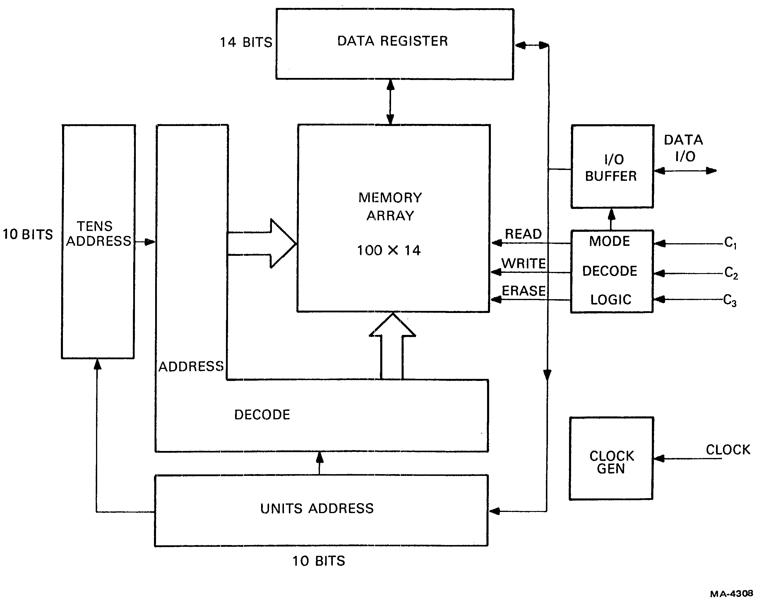
Seven states of the three control lines give commands to the NVR device:
| State | Data Bus | |||
|---|---|---|---|---|
| C3 | C2 | C1 | ||
| 0 | H | H | H | Standby. The device output floats. |
| 3 | L | L | H | Accept Address. Two 1 of 10 addresses are shifted in at the clock rate. The first group is the 10’s decade and the second is the 1’s decade of the 1 of 100 word address. |
| 2 | H | L | H | Erase. The word stored at the addressed location is erased to all zeros. |
| 7 | L | L | L | Accept Data. The data register accepts serial data shifted from the I/O pin. The address register remains unchanged. |
| 6 | H | L | L | Write. The word contained in the data register is written into the location designated by the address register. |
| 4 | H | H | L | Read. The addressed word is read from memory into the data register. |
| 5 | L | H | L | Shift Data Out. The output driver is enabled and the contents of the data register are shifted out. |
| 1 | L | H | H | Not Used. |
Several factors in the ER1400’s design require special treatment by its support circuitry. It requires 35 volts for the write and erase processes. Its signal levels are specified to be Vss (the positive power supply) for the high level and 12 volts lower than that for low. The logic of these signals is negative: 1 is asserted as a low level, and 0 is asserted high. When driving data, the NVR’s output actually switches between +12 and -23 volts with a high impedance in series with the negative source. This requires that an external clamping diode (D4) be present to pull the low level up to ground through the high impedance. 12 volts and ground are thus the I/O logic levels. The terminal controller is made with TTL, so open collector buffers with pull-up resistors to +12 volts are the interface.
The Standby command of the ER1400 is not used in the VT100. Instead, Accept Data serves as the command to the NVR during idle periods. The code for Accept Data is all inputs low. This arrangement protects the contents of the NVR from spontaneous writes that might occur due to the power-down behavior of E29, the 7417 open-collector buffers. E29, in powering down, tends to drop its outputs from the high to the low state in an unpredictable order. This could present a write command to the NVR before the power supply voltages drop low enough, if the NVR had been maintained in the Standby mode by keeping its inputs high. By keeping all outputs low with the Accept Data command, no new command can occur accidently during power-down.
The pull-up resistor used to drive the data input is too low an impedance for the ER1400 output to drive. Line C2 is high during state 5 when the output driver is enabled, and low when data is being input to the NVR, so transistor Q1’s base is connected there. When the line goes high, Q1 turns off, raising the impedance at that point to the leakage values of Q1 and E29, and the input impedance of comparator E48. D4 clamps the output to -0.6 volts to protect the comparator input from leakage to -23 volts in the ER1400.
Later VT100s may have power down circuitry in series with the Vgg pin on the ER1400 to ensure that the -23 volt supply is cut off when the +5 volt supply is low. This would prevent writing during power-down.
The comparator is a high impedance load for the ER1400 output driver and is biased to switch at +8 volts. This threshold ensures that a wide range of output levels will still pull the low state down enough to switch the comparator. The comparator output, pulled to +5 volts by a resistor, provides the NVR DATA bit to the flag buffer. The microprocessor reads the flag buffer after it sees the NVR clock flag change, and samples the NVR DATA bit to get the serial data.
The NVR clock is the lowest frequency line buffer address signal and occurs at the horizontal line rate, 15734 kHz. This is the bit shifting rate during address and data transfers. A read operation requires only a single clock cycle to transfer data into the data register but an erase or write of a word each takes 20 milliseconds.
During an NVR operation, the microprocessor uses 21 bytes of scratch pad memory to set up a group of NVR address or data bits. Each group consists of 20 bits of address or 8 bits of data with another 6 bits of fill for the 14 bit NVR word. These groups must enter the NVR serially with precise timing. The microprocessor cannot calculate the groups fast enough to keep up with the shifting process while also managing the shifting process, so it saves time by precalculating and storing each group of bits. Then it reads the stored groups, and delivers them to the NVR at the NVR clock rate through the NVR latch.
The microprocessor serializes its data by rotation in a register. It combines the data with command bits to control the NVR device. Output from the microprocessor reaches the NVR through the NVR latch. The latch is updated at each clock during an NVR operation. One unrelated signal from the communication port is routed through an extra bit in the NVR latch device.
The microprocessor reads the NVR during the power-up process. The bits are deserialized by rotation as they are read in. Although 14 bits from each NVR word are written or read, only 8 bits are used by the microprocessor. The data goes into location in the scratch portion of RAM for use during a later portion of the power-up.
Use of the ER1400 in the VT100 takes place during normal operation of the video circuits. The 8080 must be free to operate on every scan line in order to load data and address and shift data out (the ER1400 is clocked at the horizontal rate and this signal is provided as a clock to the flag word for the 8080). Because of the above two conditions, it is necessary to ensure that all DMAs performed by the video processor are short.
The processor works fast enough to permit the display of the short message “WAIT” at the left edge of the screen. This causes the DMA to be longer but informs the operator during long save and recall sequences. The timing for all of these conditions is shown in Figure 4-5-2.
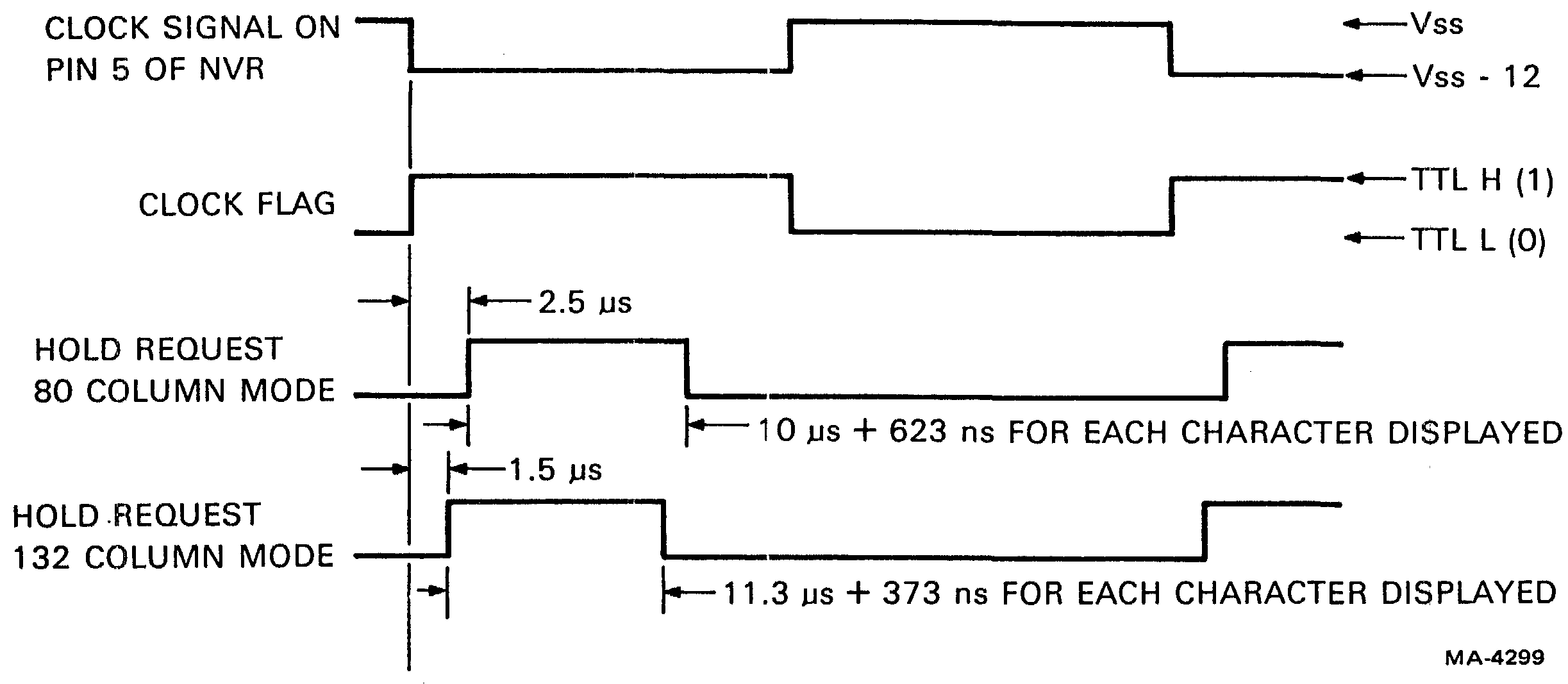
All data and command changes to the ER1400 occur immediately following the falling edge of the clock flag (the rising edge of the signal on pin 5 of the ER1400); the data is strobed into the NVR on the opposite edge. The two one-of-ten codes for address have a single zero and nine ones (at D0 of the 8080 bus).
When the “shift data out” mode is entered as per the timing diagrams in Figure 4-5-3, the first data bit may appear when the mode is entered but will become stable 25 µs later; subsequent data bits will be shifted out on the falling edge of the clock flag (rising edge of the signal on pin 5 of the chip) and will become valid 25 µs later. This means that, following a change to “shift data out” mode or a falling edge of clock flag during this mode, a delay of 25 µs must occur before reading of the NVR data flag is attempted. The first bit shifted in when writing is the first bit shifted out when reading.
When using the ER1400, it is necessary to operate with interrupts off.
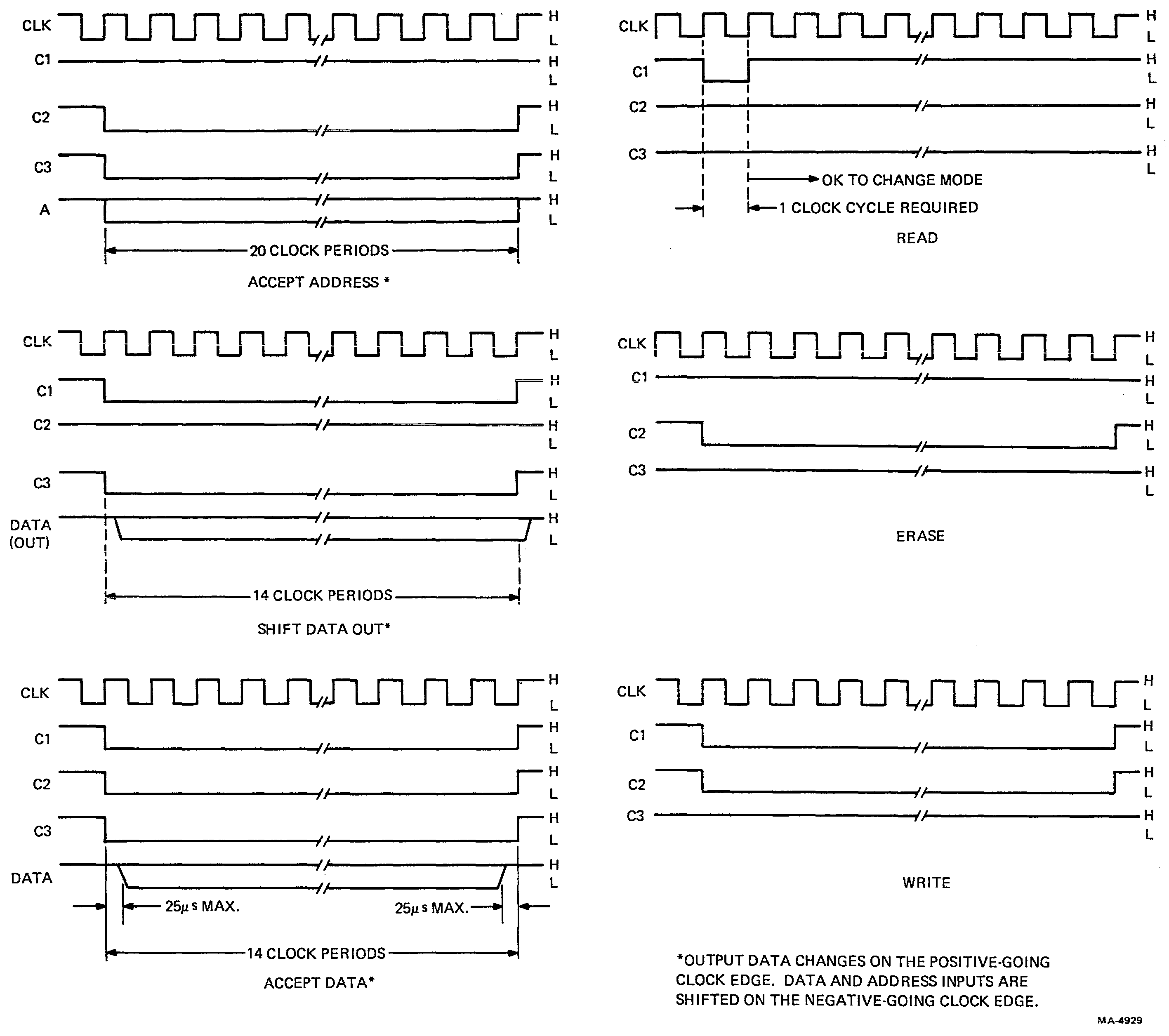
The video processor is the heart of the VT100 display. It is composed of the devices shown on the right side of the terminal controller block diagram (Figure 4-6-1). This section discusses the general mechanism that converts data into a visible display, followed by a discussion of the two central devices (the timing and control chips) followed by a general discussion of all the other blocks on the video processor side of the block diagram. The interactions between the data paths on the left of the diagram and the processor on the right are covered in Section 4.7, Microprocessor - Video Processor Interface.

The video processor converts data into an electrical signal that a CRT monitor can turn into visible letters, numbers, and symbols. The video processor works with the characteristics of the CRT monitor to do this. A brief description of these characteristics precedes an introduction to the video processor’s operation.
The raster is that area on the CRT screen that is scanned (passed over) by an electron beam moving in a regular pattern. Deflection coils cause the beam to quickly scan a series of horizontal lines while moving relatively slowly down the screen. This scanning repeats quickly and constantly, and persistence of vision makes the entire screen look continuously scanned. The beam may be on or off, lighting the fluorescent phosphor on the face of the CRT or leaving it dark, but the beam’s continuous motion traces and defines the raster.
As the beam moves in its horizontal scans, it can be turned on and off very fast. This means that a spot of light (called a dot) can be produced anywhere along each horizontal scan line. Each scan contains the same number of potential dots. If only one dot is lit in a scan but dots in the same position on several successive scans are also lit, the screen appears to have a vertical line on it. This ability to line up dots on different scans is the key operating feature of the video processor.
Limiting our discussion to 80 column lines for this description, each character that can be displayed on the VT100 is made up of a matrix of dots, ten wide and ten high (Figure 4-6-2). There are 800 dots in a scan and the raster is made of 240 scans. So there are 80 groups of ten dots in each scan horizontally, and 24 groups of 10 scans vertically. Each 10 dot × 10 scan group is a character cell, where a character can be displayed, and there are 80 × 24 character cells on the screen. As the electron beam scans the raster, the video processor turns the beam on and off, assembling the characters scan by scan.
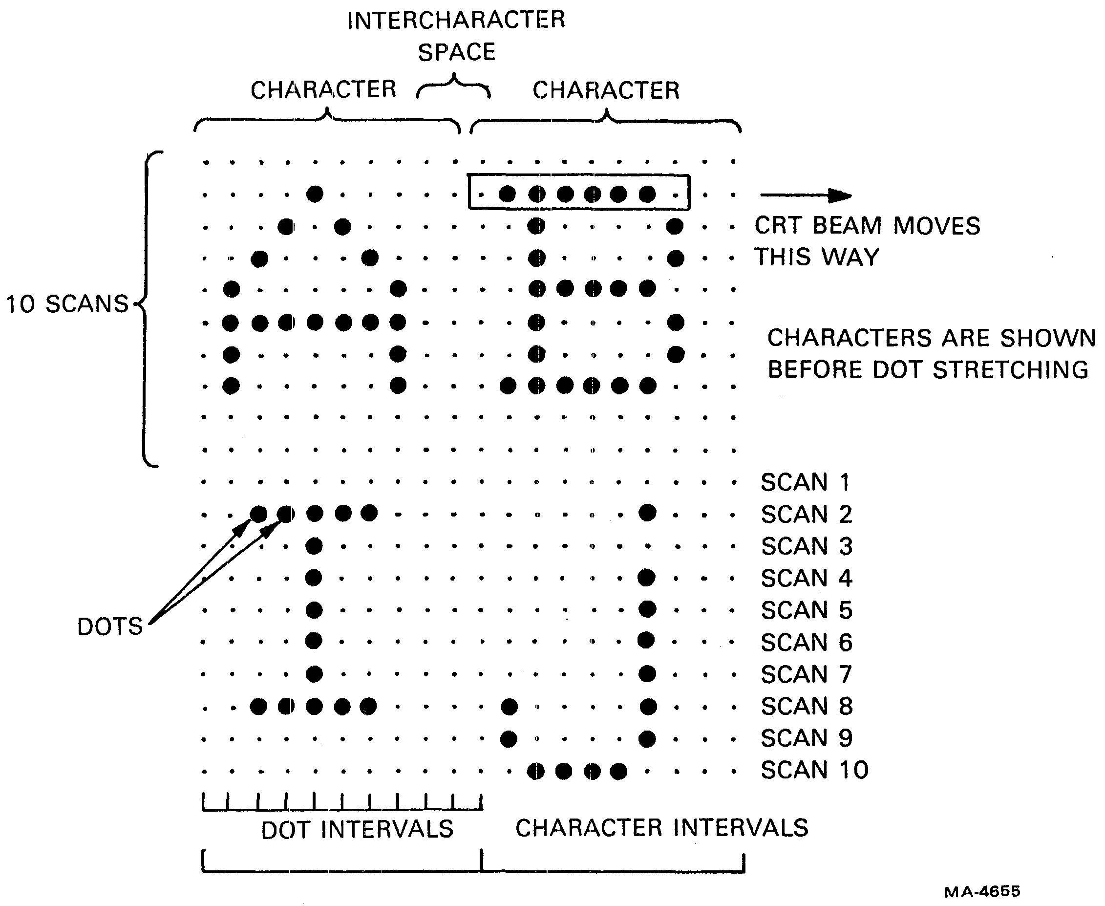
When we say the characters are assembled scan by scan, we mean that only one scan of information about a character is displayed and then the same scan for the next character is displayed. This continues to the end of a line of characters. Then the next scan of the first character is displayed, followed by the same scan of the next character, and so on. Therefore, each character must enter the video processor ten times, once for each scan, and remain only until the next character in the line is displayed.
Each character in a line is stored in one of a group of adjoining locations in the screen RAM. (See Figure 4-6-3 for the video processor functional diagram.) The process of moving a line of character data from the screen RAM to the video processor takes the same amount of time as a scan. During data movement, the microprocessor cannot use the RAM. So, to give the microprocessor as much working time with the RAM as possible, the video processor accepts the line of character data for display during the first scan and stores it in its line buffer at the same time for use during the other nine scans. Movement of data from the screen RAM to the line buffer by the video processor is called direct memory access (DMA). During the DMA, the video processor provides addresses to the screen RAM with the address counters. The data is stored in the line buffer which gets its addresses from the line buffer address (LBA) outputs from the DC011 timing chip. Both kinds of addresses change values when they receive a clock (called character clock) that occurs after each 10 dots. This clock makes the character data in the video processor change at the right times to provide proper alignment of the display.
The character latches hold the data coming from the screen RAM or line buffer and ensure that the data remains stable for long enough periods to be written into the line buffer or the video shift register. The buffer between the latches is tristatable and, during non-DMA time, prevents the normal data flow on the microprocessor data bus from interfering with the video processor’s reading of data from the line buffer.
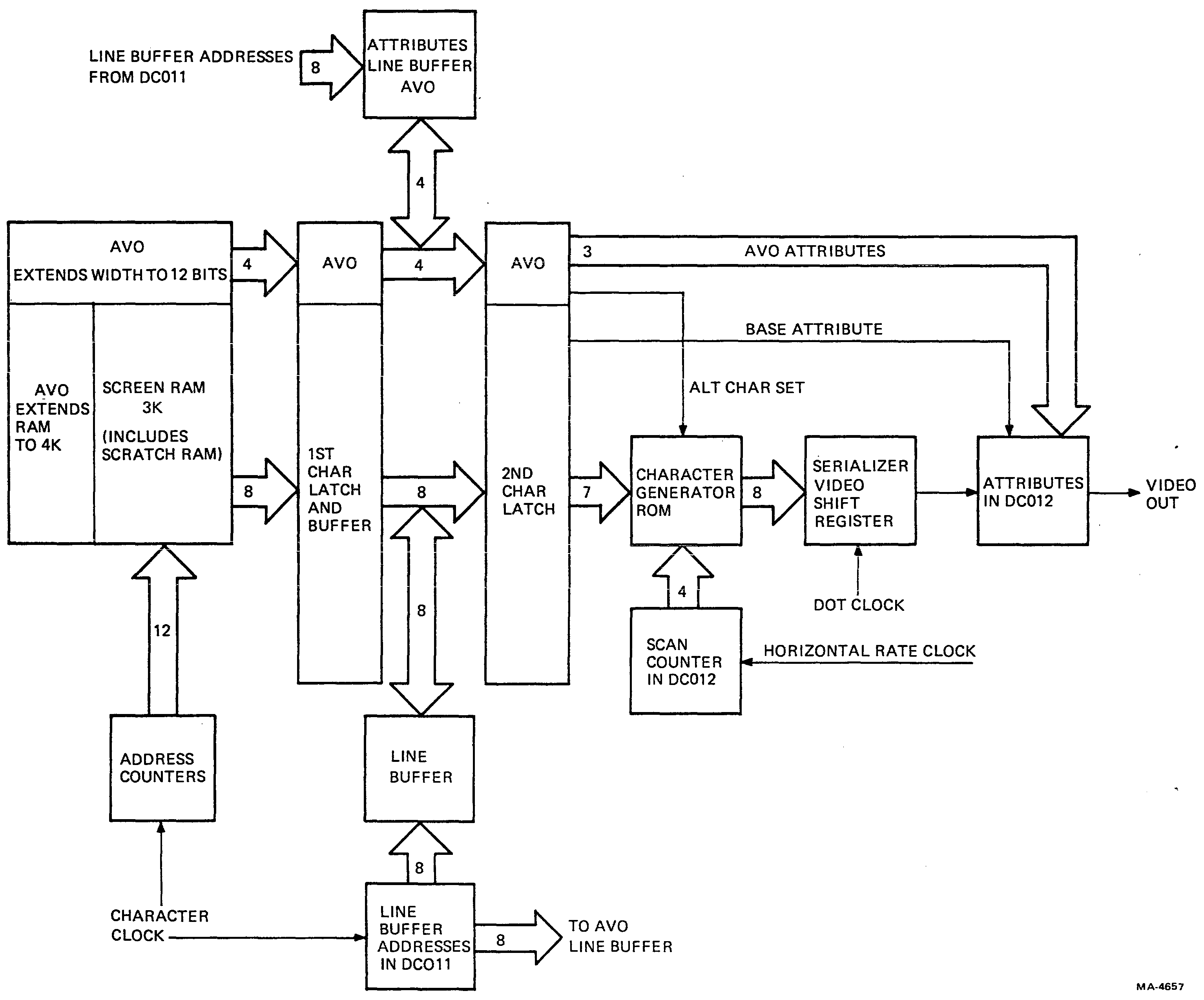
Data, coming either from the screen RAM for scan 1 or the line buffer for scans 2 through 10, becomes part of an address to a character generator ROM. (See Figure 4-6-4, Character Generator Example.) The rest of the address comes from a scan counter in the DC012 control chip. The scan counter addresses the ROM according to which of the ten scans is to be displayed. The 4-bit scan counter skips over the other 6 possible addresses to the ROM, so the ROM contains data in only 10 out of 16 locations. The output of the ROM is eight bits that represent the pattern of sequential dots to be displayed for that character on that scan. The eight bits enter the video shift register, a serializer that converts the eight parallel bits into a one-bit-wide stream. An extra flip-flop stores the last bit so it can be output to the stream two or three extra times (depending on line length) to fill the intercharacter space. The stream enters the DC012 control chip, where the final adjustments for video display are made, and then the video signal goes to the CRT monitor.
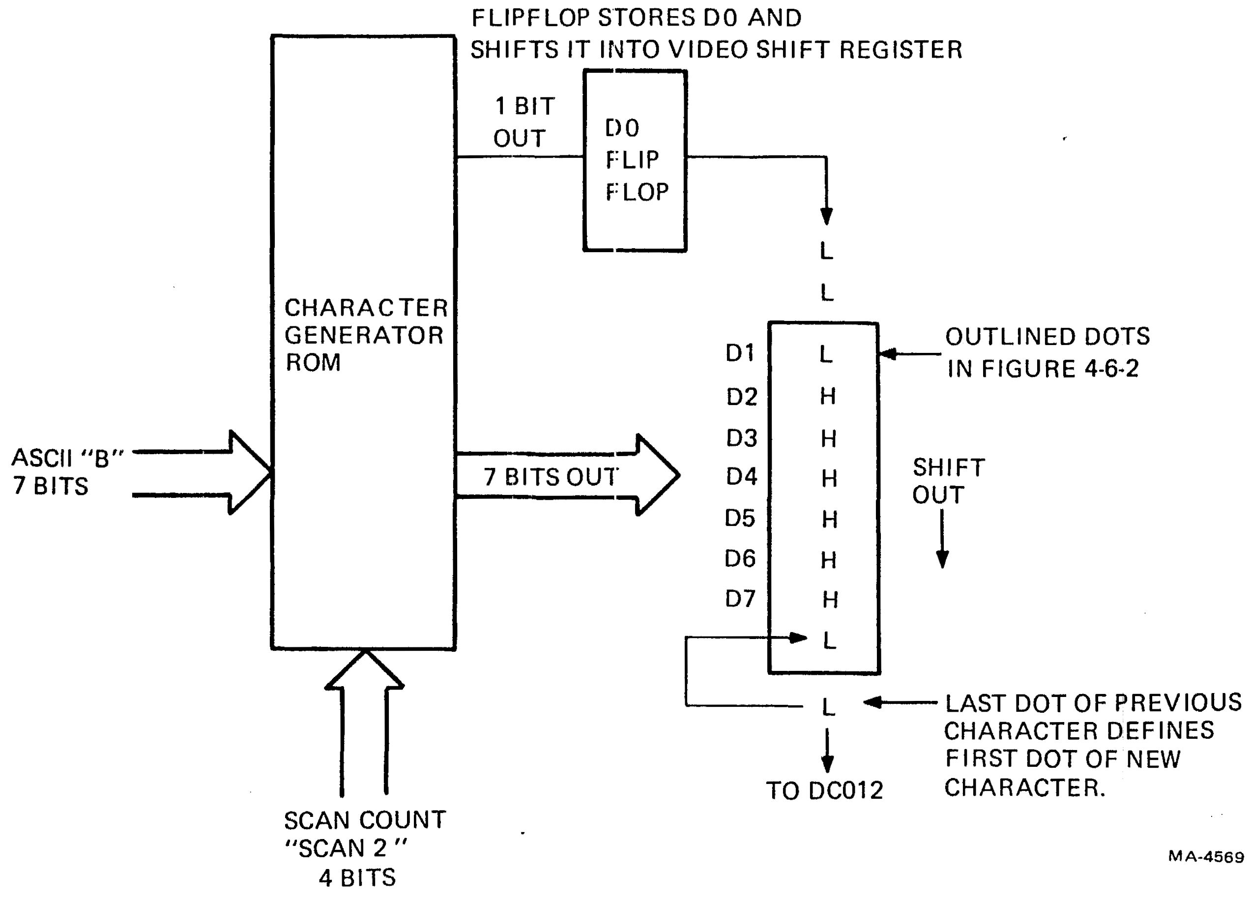
Three attributes apply to the VT100 display: character, line, and screen. Character attributes provide a special appearance to characters as they appear on the CRT screen. In the basic VT100 (without an advanced video option) only one bit of memory (called the base-attribute bit) is available to each character on the screen. The original character data from the screen RAM is eight bits wide but only seven bits define the character itself. The eighth bit defines the base attribute. The attribute bit bypasses the character generator ROM and video shift register and enters the DC012. There it controls the presence or absence of the attribute as that character is displayed. The base attribute is displayed as either reverse video or underline, depending on the selection of the cursor at SET-UP, and is invoked by the base attribute bit. Reverse video appears as all 10 scans of a character cell reversed (black changes to white and vice versa). Thus, if two vertically adjacent characters are in reverse video, no black space appears between them. Underline forces the ninth scan on (off with reverse video screen attribute.) Once a character attribute or combination of attributes is set, all displayable characters sent to the terminal have that attribute regardless of where they are placed on the screen. This continues until the attribute selection is changed.
Line attributes are double height, double width, and scroll. The VT100 displays single-width, double-width or double-height, double-width characters on a line by line basis. All characters on one line appear in the same mode. Double-width lines are generated by displaying each dot of a character twice in the horizontal direction. Double-height, double-width lines are generated by displaying each dot of a character four times (twice horizontally and twice vertically). The top and bottom halves of a double-height, double-width line must be entered as two separate lines of characters. The scroll attribute indicates that a line is part of the scrolling region.
Screen attributes affect the entire screen’s characteristics at once. They include the base attribute selection (reverse or underline as mentioned under character attributes), reverse video over the entire screen, 80 or 132 character line length, 50 or 60 Hz refresh rate (chosen according to the local power supply), interlaced or noninterlaced operation, and jump or smooth scrolling of data over the screen.
The AVO extends the length of the screen RAM so more characters can be displayed in 132 column mode. In addition, it allows each character to have four more attributes, for a total of five. Three of the AVO attribute bits enter the DC012 to control displayable features of each character. The fourth AVO attribute bit controls the selection of an extra character set by switching in an optional alternate character generator ROM that can provide non-ASCII characters or other special displays.
To provide the extra attribute bits, the AVO widens the entire screen RAM by 4 bits to make each character location 12 bits wide. It also contains a 4-bit wide extension of the character latches and a 4-bit wide attribute line buffer, addressed by the same LBA signals as the regular line buffer. This extension treats the attribute data with the same timing as the character part of the circuit, and matches each character with its attributes.
With the AVO present, reverse video, underline, bold, and blinking are all available singly or in combination. Reverse and underline appear as described above with the addition that if both reverse and underline are asserted, the underscore is forced dark instead of light. Bold increases the intensity of the display. The blink rate is about half that of the cursor or about 0.5 Hz. Cursor selection is independent of character attributes when the AVO is installed.
The DC011 is a custom designed bipolar integrated circuit that provides most of the timing signals required by the video processor. Internal counters divide the output of a 24.0734 MHz oscillator (located elsewhere on the terminal controller module) into the lower frequencies that define dot, character, scan, and frame timing. The counters are programmable through various input pins to control the number of characters per line, the frequency at which the screen is refreshed, and whether the display is interlaced or noninterlaced. These parameters can be controlled through SET-UP mode or by the host. In the following discussion, refer to the block diagram in Figure 4-6-5.
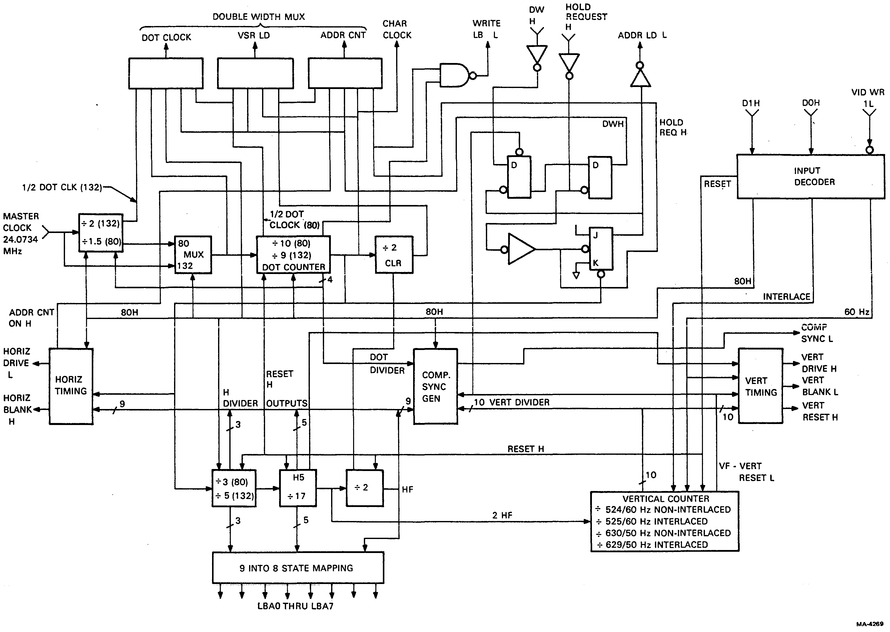
The input decoder responds to commands on the D0 H and D1 H pins (connected to D4 and D5 of the 8080 bus respectively) whenever the VIDEO WR 1 L pin is low. The outputs of the decoder select 80/132 column, 60/50 hertz refresh, and interlaced/noninterlaced modes of operation. Table 4-6-1 shows that when D1 H is low the number of columns is programmed according to the state of D0 H, and when D1 H is high the refresh rate is programmed. Interlaced mode is always selected when the column mode is set, and noninterlaced mode is selected when the refresh rate is set. The interlace mode in use depends on whether “number of columns” or “refresh rate” was selected last.
| Inputs | Configuration | ||
|---|---|---|---|
| D5 Pin 21 | D4 Pin 20 | ||
| 0 | 0 | 80 column mode | Sets interlaced mode |
| 0 | 1 | 132 column mode | |
| 1 | 0 | 60 hertz mode | Sets noninterlaced mode |
| 1 | 1 | 50 hertz mode | |
In addition to strobing data into the input decoder, VID WR 1 L also acts as a reset signal for the DC011. Whenever VID WR 1 L is low, the counters in the DC011 are held in a cleared state. Resetting the counters serves no purpose in the VT100 because the remainder of the VT100 synchronizes itself to the DC011, but a reset is useful for testing both individual chips and complete modules. Because writing into the DC011 would cause the counters to reset and disturb the display, this is never done unless the mode is being changed.
The column mode is changed by modifying the divisors of three of the counters in the DC011. The first of these counters divides the input clock (MASTER CLK) by 1.5 to produce the dot rate clock for 80 column mode. The DOT CLK output provides the signal that controls the shifting of dots out from the video shift register. A multiplexer determines what rate DOT CLK will have for the entire screen by selecting either the output of the divide-by-1.5 in 80 column mode, or by selecting the 24 MHz MASTER CLK directly in 132 column mode. The other two counters affected by 80/132 selection are the dot counter and the horizontal counter.
The dot counter uses four flip-flops to divide the DOT CLK that was selected by the multiplexer by 10, in 80 column mode, or by 9, in 132 column mode. The output of the dot counter is the character rate clock, which is used to move character codes in the latches that are outside the DC011. Character clock is further divided by the horizontal counter. The timing of CHAR CLK is shown in Figures 4-6-6 and 4-6-7 for each of the two column modes. CHAR CLK is unaffected by double-width mode. The output of the next-to-last flip-flop is used for the write enable signal for the line buffer RAMs (WRITE LB L). WRITE LB L is also shown in Figures 4-6-6 and 4-6-7. This signal allows the data and address changes, caused by the rising edge of CHAR CLK, to become stable before writing is enabled and then disables writing before CHAR CLK rises again. WRITE LB L is gated directly with HOLD REQ H so that it is active only during DMAs. Intermediate signals from the four flip-flops are used by various other functions in the DC011 such as the double-width multiplexer and the composite sync generator.
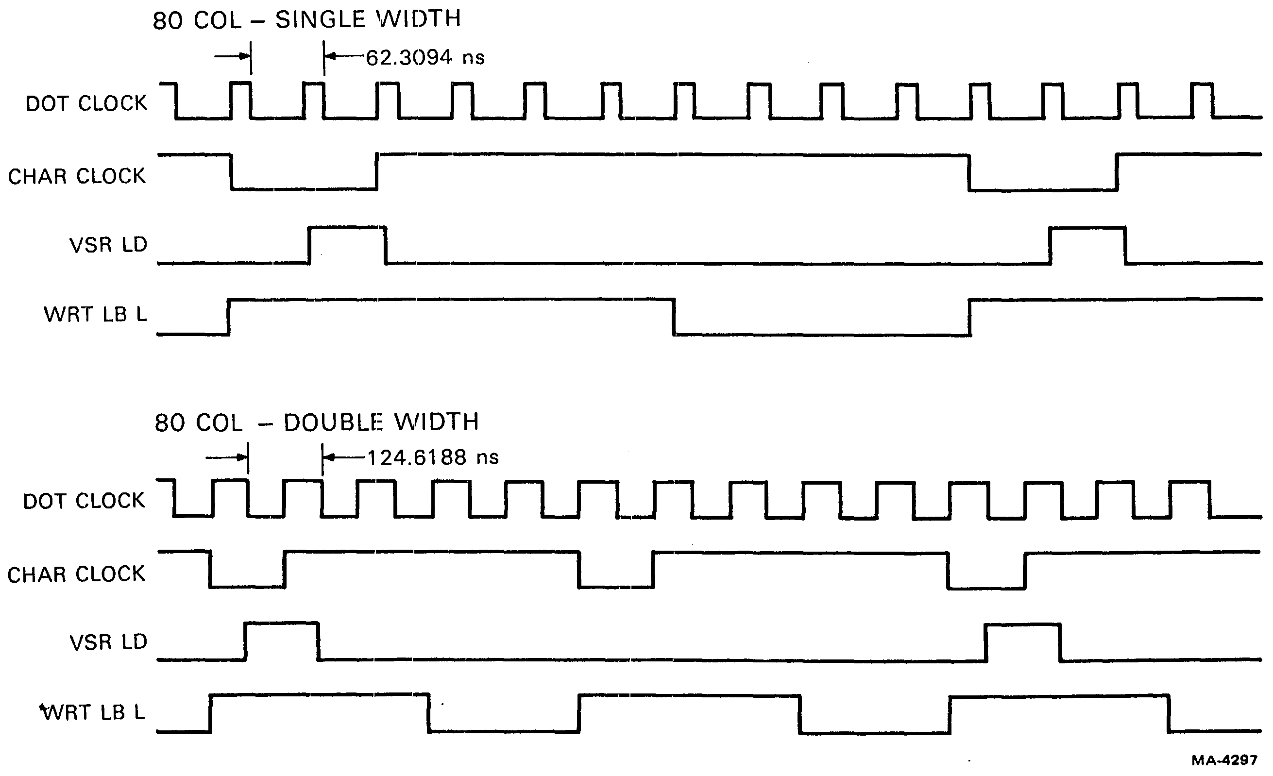
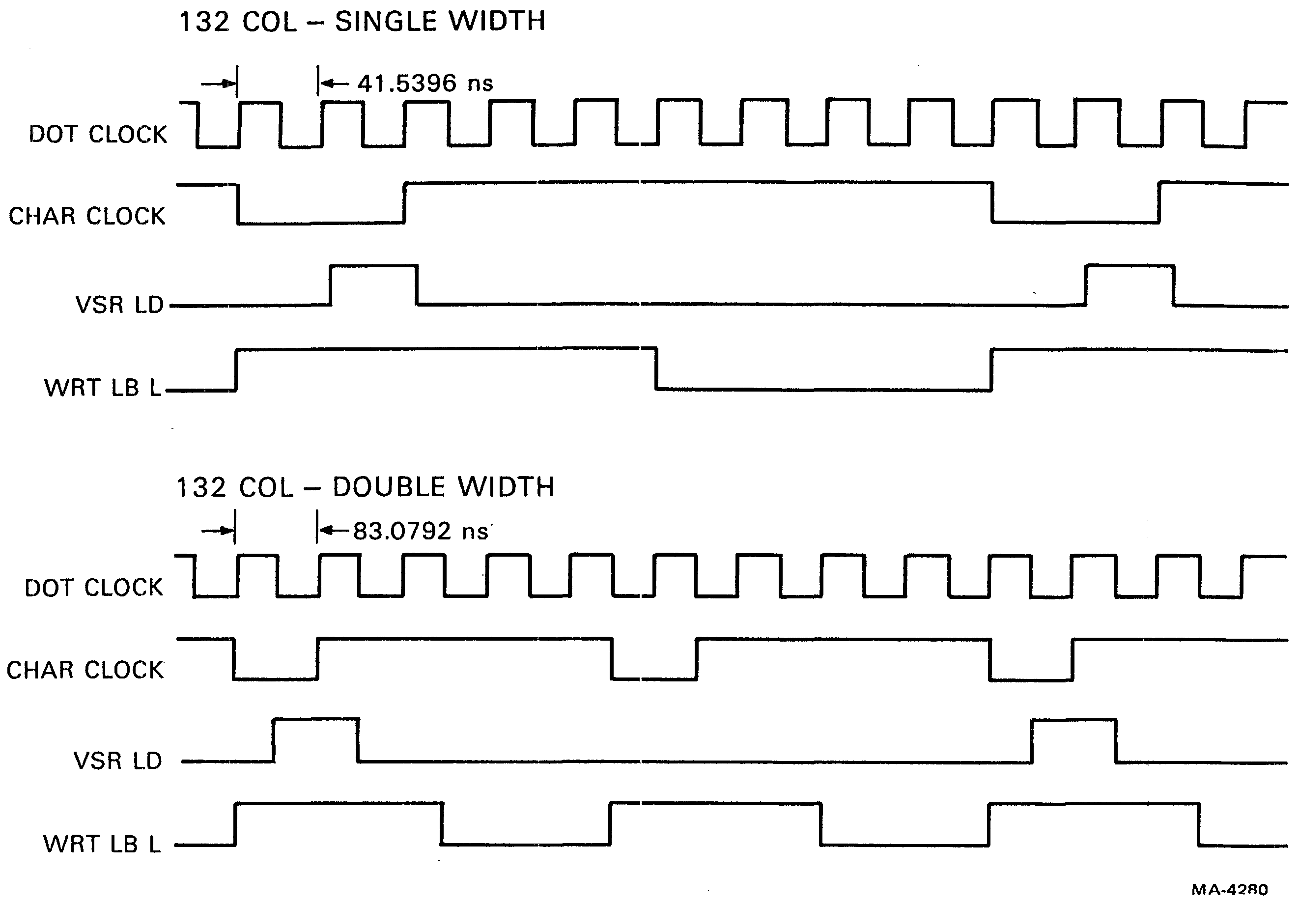
The double-width multiplexer (MUX) produces the three signals whose timing must be changed when a line of characters is switched between single- and double-width modes. The frequency of DOT CLK must be divided in half on a double-width line so that the video shift register will shift half as often, making each dot (and therefore each character) twice as wide as it would be in single-width mode. In order for the video shift register to work properly with the half-rate DOT CLK in double-width mode, the load signal for the shift register (VSR LD H) must still come every 10 dots (80 column mode) or 9 dots (132 column mode). Therefore loads must occur at every other CHAR CLK. Similarly, incrementing the DMA address counters occurs on every other CHAR CLK to ensure that characters that are stored sequentially in the screen RAM are presented to the shift register at the correct time for each VSR LD H pulse. The different modes of DOT CLK and VSR LD H are shown in Figures 4-6-6 and 4-6-7.
In single-width mode, the double-width MUX directs the output of the 80/132 MUX to the DOT CLK pin, providing either a 16 MHz or 24 MHz output. To get the half-rate DOT CLK for 80 column mode, the double-width MUX selects the output of the first flip-flop in the dot counter, that acts as a divide-by-2 because the dot counter is dividing by 10 (10 is an even number). In 132 column mode the same selection cannot be made because the dot counter is dividing by 9. But the divide-by-1.5 is not needed in 132 column mode, so this divider is converted to a divide-by-2 and the double-width MUX selects its output when a double-width line is displayed in 132 column mode.
The load input of the video shift register used in the VT100 is a synchronous input. This means that when the load input is high, the rising edge of DOT CLK causes a parallel load to be performed instead of a shift. To get one load and many shifts for each character, VSR LD H can only last for that one cycle of DOT CLK that is adjacent to CHAR CLK. Furthermore, transitions of VSR LD H must satisfy set-up and hold times with respect to the rising edge of DOT CLK. In single-width modes, VSR LD H is one dot time wide, generated from the outputs of the dot counter, and its set-up and hold times are guaranteed by internal propagation delays. This relationship is shown in Figures 4-6-6 and 4-6-7 by a slight shift in the transitions of VSR LD H with respect to DOT CLK. In double-width mode, VSR LD H is created by selecting every other CHAR CLK (Figure 4-6-5 shows a flip-flop that divides CHAR CLK by two for this purpose) and then delaying this signal by one single-width dot time.
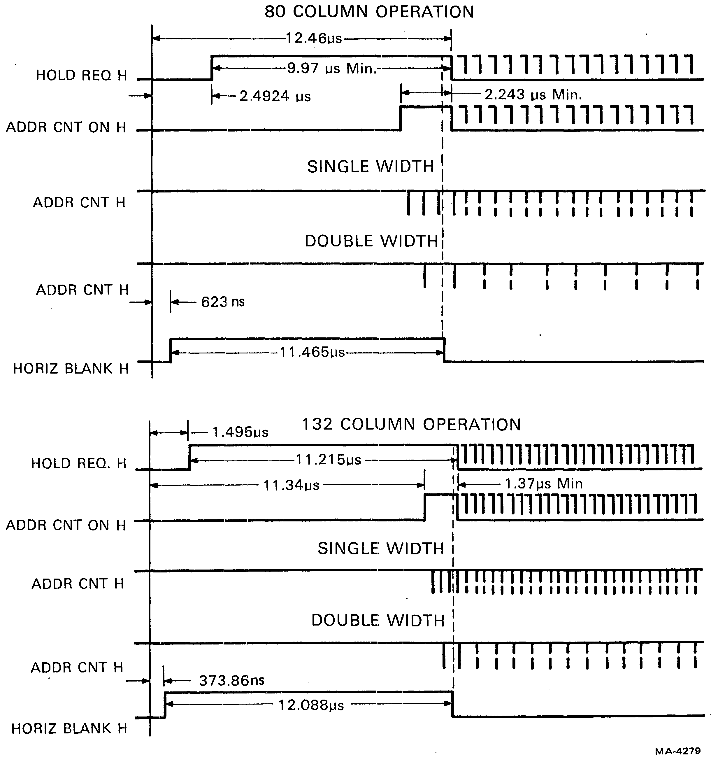
The signal that increments the DMA address counter (ADDR CNT) is shown in Figure 4-6-8. ADDR CNT has the same timing as CHAR CLK; the difference is that it does not run continuously. Figure 4-6-8 shows that ADDR CNT can only be generated if HOLD REQUEST H is high and that it is further controlled by a signal from the horizontal timing section (ADDR CNT ON H) that allows ADDR CNT to provide exactly three pulses (in single-width mode) before HORIZ BLANK H goes low. The three pulse delay primes the external character latches so that the dots for the first character on a line are being loaded into the video shift register at the same moment that HORIZ BLANK H enables the video at the beginning of a scan. The only change made to ADDR CNT for double-width operation is that every other pulse is deleted, beginning with the first pulse (Figure 4-6-8).
The block diagram in Figure 4-6-5 shows the horizontal divider broken into three stages. The first divider is programmable according to the number of columns selected and is driven by CHAR CLK from the dot counter. For 80 column mode the divisor is three; for 132 column mode the divisor is five. The total division from MASTER CLK to the output of this first divider is 45, independent of mode (for 80 columns: 1.5 × 10 × 3 = 45, for 132 columns: 1 × 9 × 5 = 45). Therefore, the operation of all of the remaining dividers in the DC011, which are driven from the first horizontal counter, are also independent of the column mode. The second stage of the horizontal divider has a divisor of 17, which is chosen to give the required number of displayable columns plus about 28 percent more to allow time for the monitor to execute a horizontal retrace. The last stage is a simple divide-by-2 that provides the horizontal frequency. Designing the last stage to be a divide-by-2 guarantees that the signal at its input will have a frequency twice that of the horizontal frequency as required by the vertical dividers to create interlaced operation. The total division from CHAR CLK provided by the horizontal divider is 102 in 80 column mode and 170 in 132 column mode. In either mode the frequency at the output of the horizontal counter is 15.734 kHz.
Two timing signals are generated from the horizontal counter to control those system functions occurring at the scan rate. These signals begin at the end of a scan and last until the horizontal counter is incremented past a specific state that is decoded to turn the signals off. The monitor requires a pulse at the end of every scan to tell it when to initiate a retrace and begin the next scan; the duration of this pulse must be between approximately one-quarter and one-half of one scan. Figure 4-6-9 shows HORIZ DRIVE L as produced by the DC011; the slight difference in timing between 80 and 132 column modes is the result of design convenience and is not significant to the operation of the VT100. HORIZ BLANK H is designed to allow 83 characters during the forward scan in 80 column mode and 137 characters in 132 column mode. The extra characters are included for possible future use such as a field of indicators along the right margin of the screen or as extra symbols inserted to mark text. The rising edge of HORIZ BLANK H is synchronized to CHAR CLK to eliminate the accumulated delay of the horizontal counter. The falling edge of HORIZ BLANK H occurs between two CHAR CLKs (Figure 4-6-8) to meet some requirements of the DC012, but inside the DC012 HORIZ BLANK H is delayed to the following edge of CHAR CLK so that the beginning of each displayed scan will coincide with a character boundary. The actual video blanking occurs inside the DC012. Therefore there is no signal outside the DC012 that has the exact length of horizontal blank time.
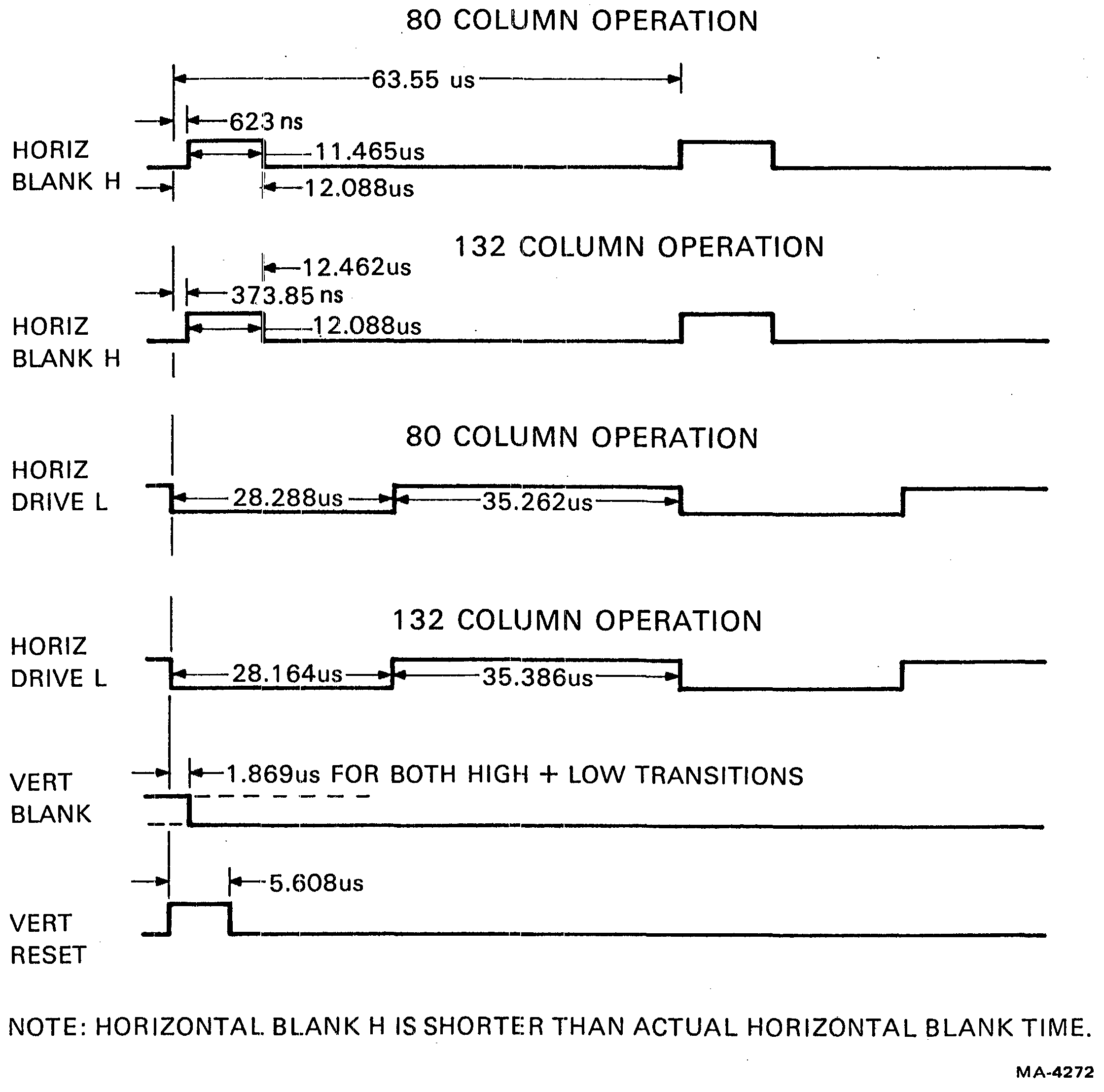
The line buffer memory stores one line of characters during a scan on which a DMA occurs and then recalls these characters on each successive scan until the next DMA. Because the line buffer is a random access memory, it has address inputs that must be provided with a sequence of addresses that change at each CHAR CLK such that each character is stored in a unique location. The horizontal counter can provide such addresses because it is incremented through a series of unique states that repeat in the same sequence on every scan. Because of the three stages that comprise the horizontal counter, there are nine flip-flops whose outputs must be converted into the eight line buffer address (LBAs) outputs. The conversion is possible because the 9 flip-flops represent a maximum of 170 states in 132 column mode (8 bits can represent 256 states). The DC011 contains gates that combine the output of the ninth flip-flop in the horizontal counter with the outputs of the other eight to generate some addresses that are not otherwise represented by the eight. The resulting LBAs do not follow a normal binary counting sequence but the sequence of unique addresses repeats exactly on each scan. Figures 4-6-10 and 4-6-11 show the LBA sequence for one-half of a scan; the other half is identical except that LBA 7 is low.
Several of the LBAs are used as general purpose clocks in the VT100. LBA 3 and LBA 4 are used to generate timing for the keyboard. These signals satisfy the keyboard’s requirement of two square-waves, one twice the frequency of the other, even though every 16th transition is delayed (the second stage of the horizontal counter divides by 17, not 16). LBA 7 is used by the nonvolatile RAM. The 31.468 kHz signal on LBA 6 could be used for power supply synchronization, although this is not done in the VT100.
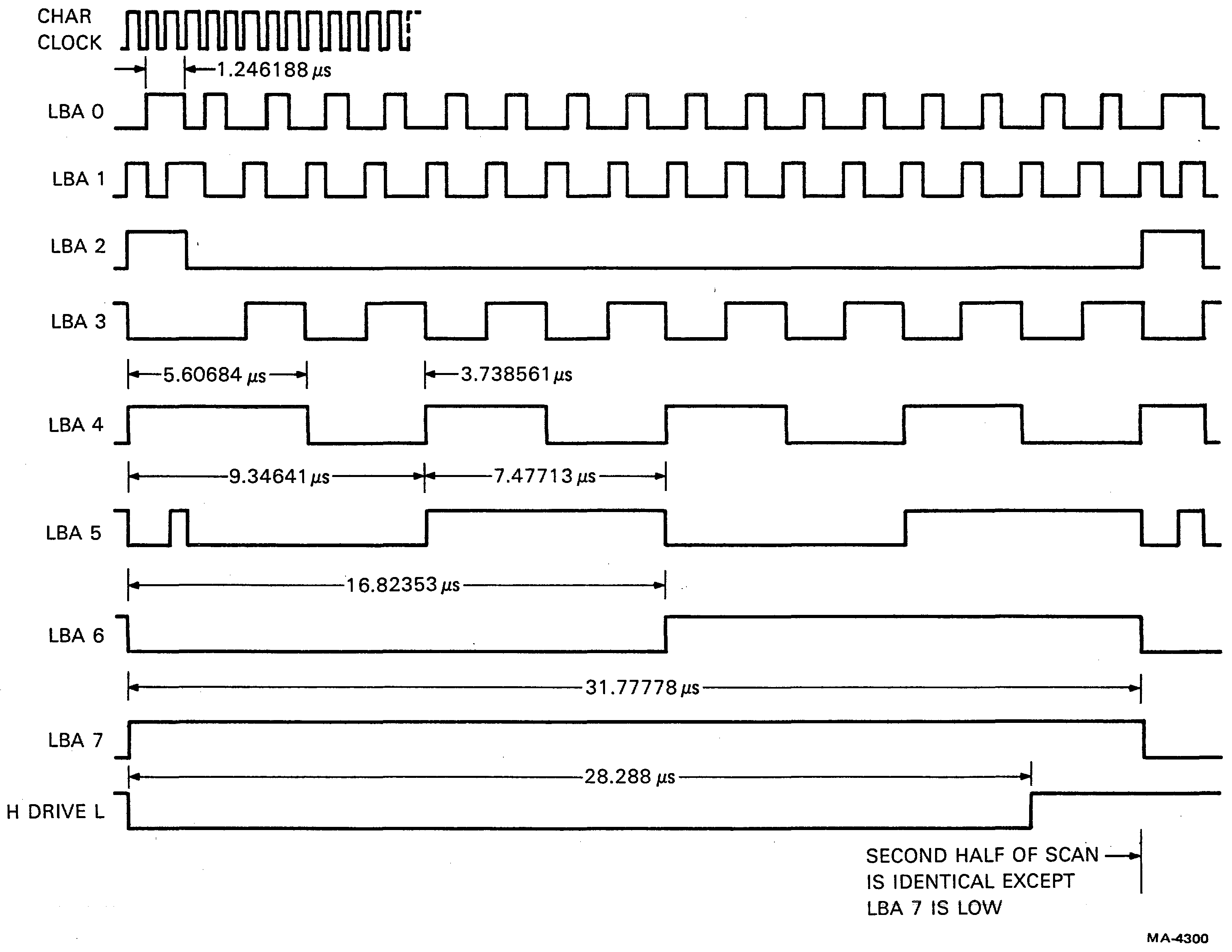
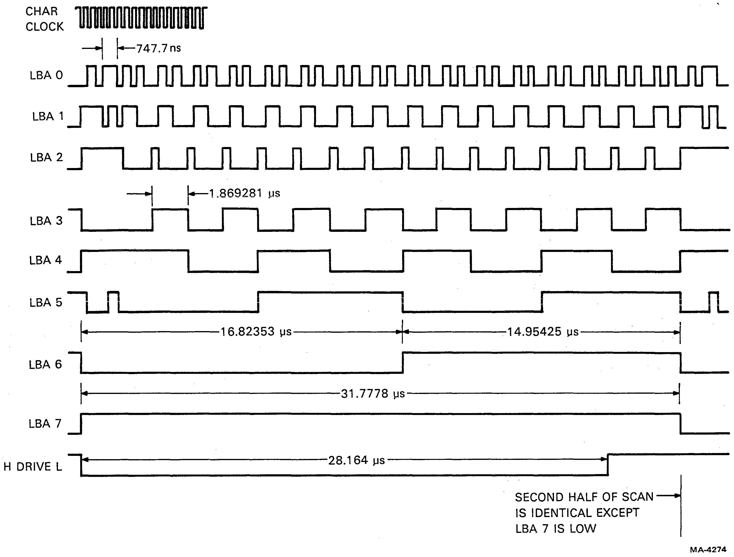
To paint a complete picture on the screen, the monitor moves the electron beam slowly from the top of the screen to the bottom, while it is also moving the beam quickly from left to right to paint each scan. The vertical sweeps of the beam must be repeated continuously so that the picture is refreshed often enough to prevent the appearance of flicker. In television terminology, a single pass of the beam from the top of the screen to the bottom (and the data displayed during that time) are referred to as one field. A complete picture, which may contain one or more fields depending on the type of interlacing in use, is called one frame. When the VT100 is used in noninterlaced mode, each successive field is identical and therefore only one field is contained in each frame. During interlaced operation in the VT100, there are two types of fields that alternate with each other so that each frame consists of two fields. Even fields start at the top of the screen and display 240 scan lines before reaching the bottom. Odd fields place their first scan line between the first and second scans of the preceding even field and then place each additional scan between succeeding scans of the even field. Interlacing the even and odd fields gives a whole frame of 480 scans, instead of 240 scans, to provide increased vertical resolution. In noninterlaced operation, commands to the monitor to begin a new field are always coincident with commands to begin a new scan. This causes the beam to always be in the same vertical position when the first displayed scan is begun. But, in interlaced mode, odd fields begin with a command for a new frame that occurs halfway through a scan line. This causes the beam to have moved down the screen from where it would have been during an even field (by the distance that it moves in one-half of a scan) when the first displayed scan is begun. Even and odd fields are made to alternate by including an odd number of half-scans in every field. This is in contrast to noninterlaced operation, where each field contains only complete scans. The VT100 always displays the same video information on both even and odd fields. Interlaced mode is provided for future use by options that desire increased vertical resolution.
The 10-bit vertical counter, shown in Figure 4-6-5, determines the frequency at which the screen is refreshed by counting the number of horizontal scans to be included in each field. The vertical counter uses the 31.468 kHz output of the horizontal counter so that it can count the half-scans required for interlaced operation. Figure 4-6-5 lists the four available divisors that select the interlace mode and keep the refresh frequency as close to the local power line frequency as possible (to minimize interference with the screen from nearby equipment). The vertical frequencies produced by these divisors are approximately 1/20 Hz above or below the nominal power line frequency.
Three outputs are derived from the flip-flops in the vertical counter to control the vertical refresh operations in the VT100. These signals are shown in Figures 4-6-12 and 4-6-13 for all four modes. VERT DRIVE H is issued at the bottom of the screen to initiate a vertical retrace followed by a new vertical scan. This operation is analogous to the effect of HORIZ DRIVE L on horizontal scans. The time between any two VERT DRIVE Hs is a constant, equal to an even number of half-scans in noninterlaced mode and equal to an odd number of half-scans in interlaced mode. VERT BLANK L always enables exactly 240 scans during any field and blanks any remaining scans. Furthermore, VERT BLANK L is always turned off exactly 20 scans after VERT RESET H in 60 Hz mode and 50 scans after VERT RESET H in 50 Hz mode. VERT BLANK L is always adjusted to display complete scans even during odd fields in interlaced mode. VERT RESET H initiates the DMA process at the start of every field. When VERT RESET H goes high, the DMA address counters are reset to point to address 2000H in the screen RAM, all line attributes are cleared, and the scroll counter in the DC012 is preset to the value stored in the scroll latch. (See the DC012 description for more explanation.) During noninterlaced operation and on even fields, VERT RESET H occurs at the same time as VERT DRIVE H; but, on odd fields VERT RESET H is delayed one-half of a scan to match the start of a horizontal scan. The relationship of VERT RESET H and transitions of VERT BLANK L to HORIZ BLANK H and HORIZ DRIVE L is depicted in Figure 4-6-9. Notice that VERT BLANK L always turns on or off when the video is already blanked by HORIZ BLANK H.
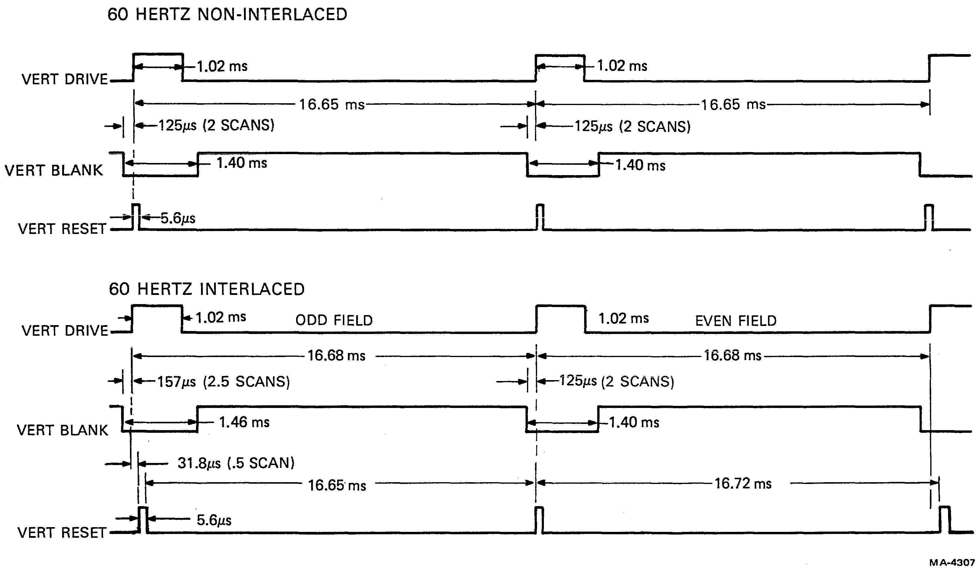
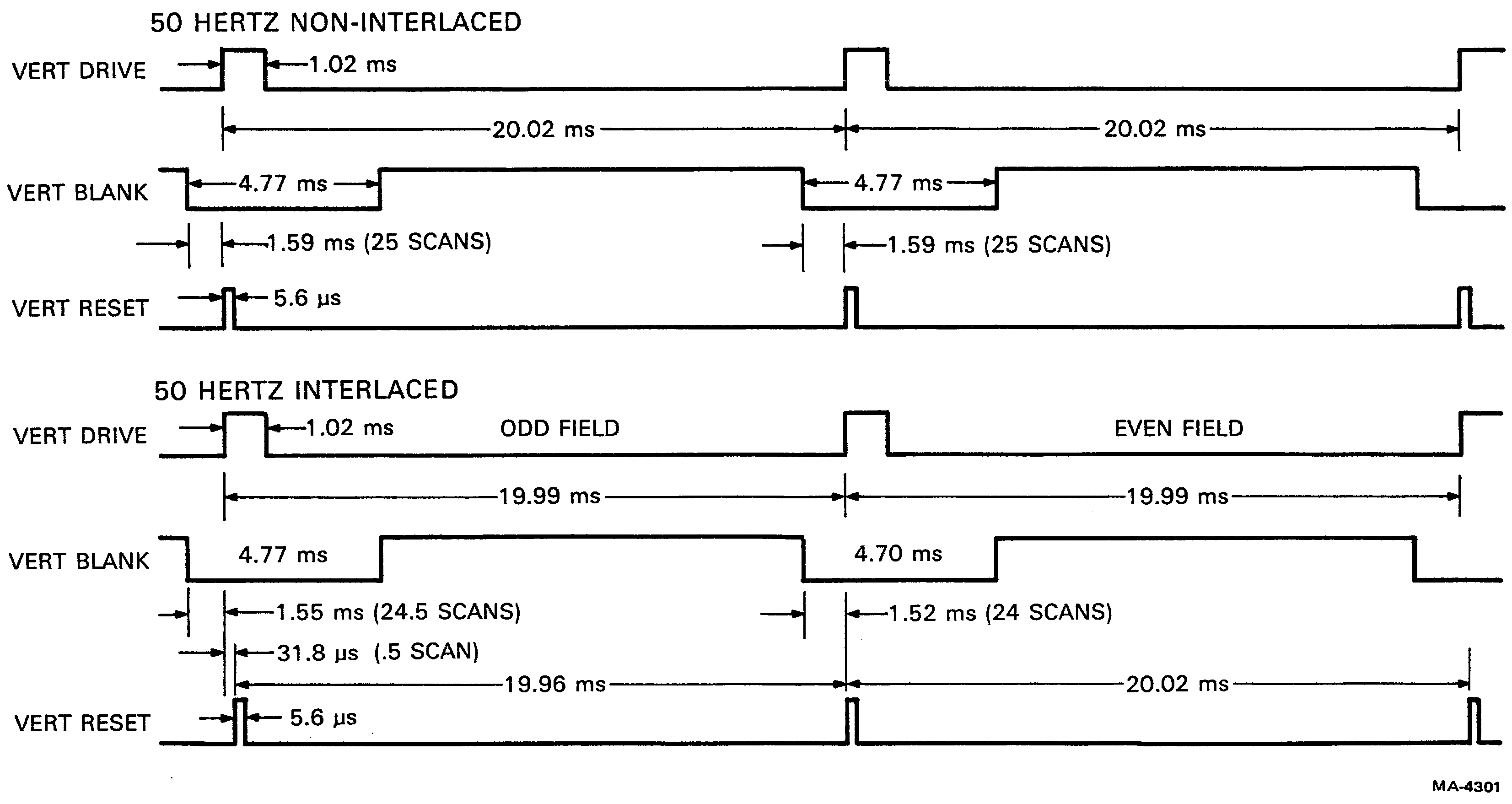
The COMP SYNC L signal supplied by the DC011 is combined with video information by the terminal controller board to produce the composite video signal that appears on J9 at the back of the VT100. An external monitor can use the composite video signal to reproduce the image displayed on the VT100 screen. This is accomplished by using the video information to control beam intensity and the composite sync waveform to synchronize the raster to the video information. The composite sync generator in the DC011 uses outputs from the dot, horizontal, and vertical counters to generate the complex timing of COMP SYNC L. COMP SYNC L consists of one of the vertical intervals depicted in Figure 4-6-14 followed by 240 horizontal sync pulses, another vertical interval, etc. The vertical synchronizing interval consists of a transition from horizontal sync pulses to six equalizing pulses, six vertical sync pulses, six more equalizing pulses, and then a return to horizontal sync pulses. Two vertical intervals are shown in Figure 4-6-14. The vertical interval that begins an odd field is similar to that which begins an even field except that the equalization and vertical sync pulses are shifted by one-half scan with respect to the horizontal sync pulses. In noninterlaced mode all fields are even fields; but, in interlaced mode every other field is an odd field. Figure 4-6-14 also shows the relationship of COMP SYNC L to both the horizontal blank time (HORIZ BLANK H modified by the DC012) and VERT BLANK L. COMP SYNC L meets the requirements of EIA RS-170 and the NTSC standards for sync pulse generators.
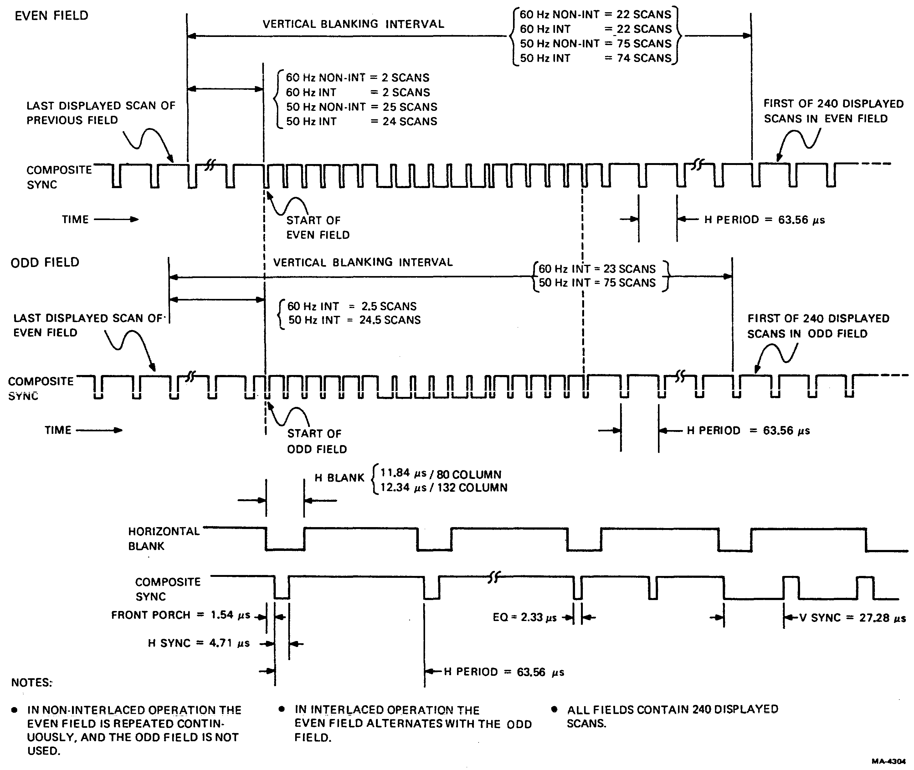
The logic associated with HOLD REQ H, ADDR LD L, and DW H is shown in Figure 4-6-5. The falling edge of HOLD REQ H sets ADDR LD L to the low state; ADDR LD L is subsequently cleared by the falling edge of CHAR CLK, thus creating a short low pulse on ADDR LD L at the end of each DMA. ADDR LD L stores, in their respective registers, all line attributes and the memory address of the next line to be accessed by a DMA. The rising edge of HOLD REQ H causes the value of DW H that was stored in the holding flip-flop by the previous ADDR LD L to be transferred to a second flip-flop whose output controls the double-width MUX. This means that the value of DW H stored at the end of one DMA by ADDR LD L does not actually become effective until the beginning of the next DMA. The holding flip-flop for DW H is cleared by VERT RESET H at the start of every field. HOLD REQ H is also used to enable ADDR CNT and WRITE LB L only during DMAs. Interactions of HOLD REQ H with other signals during a DMA are further defined in Figure 4-6-19.
The control chip (DC012), like the timing chip, is a custom bipolar device. It accepts attribute specifications and timing signals and delivers addresses for the character generator ROM and attributes for the video output to the monitor. It also generates the HOLD REQUEST signal that halts the microprocessor and initiates DMAs to get lines of characters. Refer to the block diagram, Figure 4-6-15.
The DC012 performs three main functions.
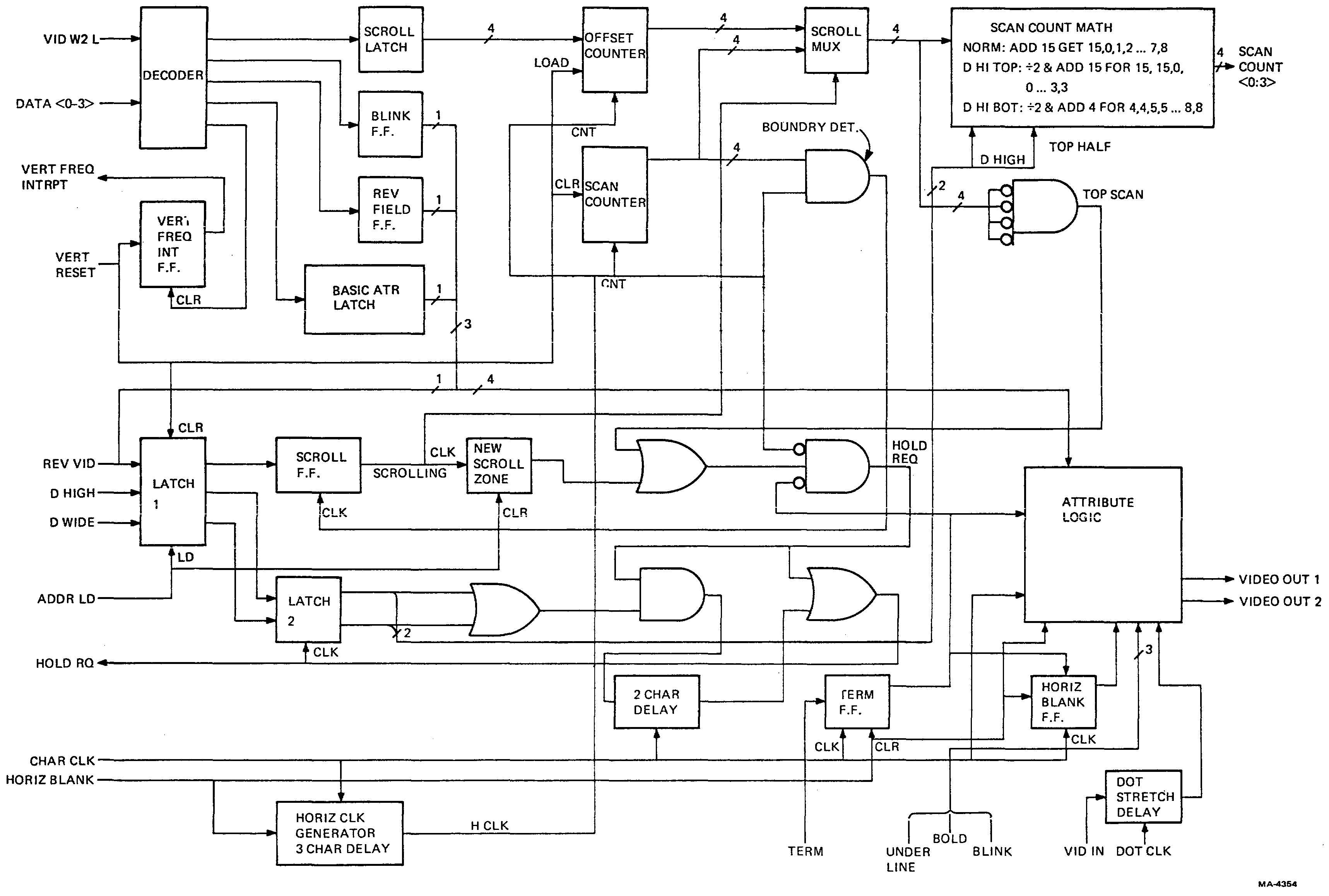
The input decoder accepts a 4-bit command from the microprocessor when VID WR 2 L is asserted. Table 4-6-2 lists the commands.
The low eight values are used to load the scroll latch with the offset for smooth scroll. The scroll latch is loaded in two passes, first writing the two least, and then the two most significant bits. Because the offset is a decimal value controlling 10 display scans, the combination setting the most significant bits to 11B is not used in the VT100 (11B covers the range 12-16).
The input decoder also toggles the blink flip-flop by complementing the state of the flip-flop whenever 1000B is written. The blink flip-flop invokes blink only where the blink attribute is set.
To save external hardware the vertical frequency interrupt flip-flop is located in the DC012 because a spare pin was available. It is set by the falling edge of Vertical Reset. It is cleared by writing 1001B into the input decoder.
Set and clear of reverse field are not toggled because the absolute state is important and there is no feedback for the system to detect the current state. Therefore, the two states are explicitly set to their desired values.
1100B means set base attribute to underline and 1101B means set base attribute to reverse video. 1110B and 1111 B are for future specification.
Any time the input decoder is loaded with 11XXB, the blink flip-flop gets cleared. This is the only way to initialize blink in the chip testing process. The firmware does not currently use the ability to clear the blink flip-flop but if hardcopy output was being implemented, it could be used to set the blink to a known state during a freeze.
| D3 | D2 | D1 | D0 | Function |
|---|---|---|---|---|
| 0 | 0 | 0 | 0 | Load low order scroll latch = 00 |
| 0 | 0 | 0 | 1 | Load low order scroll latch = 01 |
| 0 | 0 | 1 | 0 | Load low order scroll latch = 10 |
| 0 | 0 | 1 | 1 | Load low order scroll latch = 11 |
| 0 | 1 | 0 | 0 | Load high order scroll latch = 00 |
| 0 | 1 | 0 | 1 | Load high order scroll latch = 01 |
| 0 | 1 | 1 | 0 | Load high order scroll latch = 10 |
| 0 | 1 | 1 | 1 | Load high order scroll latch = 11 (not used) |
| 1 | 0 | 0 | 0 | Toggle blink flip-flop |
| 1 | 0 | 0 | 1 | Clear vertical frequency interrupt |
| 1 | 0 | 1 | 0 | Set reverse field on |
| 1 | 0 | 1 | 1 | Set reverse field off |
| 1 | 1 | 0 | 0 | Set basic attribute to underline* |
| 1 | 1 | 0 | 1 | Set basic attribute to reverse video* |
| 1 | 1 | 1 | 0 | Reserved for future specification* |
| 1 | 1 | 1 | 1 | Reserved for future specification* |
| *These functions also clear blink flip-flop. | ||||
The line attributes are managed by two latches that store the scrolling, double height (DH), and double width (DW) bits. The first latch stores the incoming data when Address Load (ADDR LD) goes low at the end of a DMA. Scrolling means that the next line will be part of the scrolling region, DH means the next line will be double height, and DW specifies top or bottom half for double-height lines. There is no double height, single width combination, so in double height, double width is assumed. The DW pin also tells the DC012 to extend HOLD REQUEST during double width. The second set of latches for double width and double height are clocked by the rising edge of HOLD REQUEST (similar to the second latch for double width in the DC011) to invoke the attributes at the beginning of the new line. The first latch stores those attributes from the end of one DMA to the beginning of the next. It is the outputs of the second latch that invoke attributes in the chip. The scroll bit is invoked by a different signal that will be discussed later. The pin defining scrolling is the same pin as reverse video; it means scrolling when loaded in by ADDR LD L and it means reverse video at all other times. The reverse video signal passes from the input pin around the first latch directly to the attribute logic.
The scroll counter consists of two 4-bit, divide-by-10 counters called the Scan counter and the Offset counter. Both are clocked at the horizontal rate to count scans. The Scan counter is cleared by VERTICAL RESET so that it starts at 0 and counts by 10s down to the end of the screen.
The Offset counter is loaded with the contents of the scroll latch by VERTICAL RESET. The Scroll latch is loaded by the microprocessor and defines the offset between the Scan and Offset counters for an entire frame because the Offset counter is only loaded at vertical reset time. The microprocessor will load the latch with the offset for the next frame during the current frame.
At the beginning of a frame, the two counters divide by 10 but start at different numbers. If not currently scrolling, the offset is 0 and there is no functional difference between the counters. If in the middle of a smooth scroll, the offset will be some other value from 1 to 9. The scan address outputs from the chip to the character generator ROM are either the output of the Offset counter or of the Scan counter, depending on whether the current line is in or out of the scrolling region, respectively. One of the two counters is selected by a 4-bit wide multiplexer (MUX) whose output is the Counter In Use. The MUX is controlled by the scroll flip-flop which is the second latch for the scroll attribute bit. Most line attributes (double height, double width) take effect when HOLD REQUEST goes high for the line in which they are effective. They always take effect with the actual data being displayed. However, the scroll flip-flop can only change state when crossing one of the fixed 10 scan boundaries that are defined by the Scan counter reaching 0.
Each scan when the Scan counter reaches 0 is a scan on the screen where a change can occur from a nonscrolling to a scrolling region, or from a scrolling to a nonscrolling region since this is normally where one line of data changes to the next if the line were not scrolling. This is the only place changes can occur because the bottom of a nonscrolling line of characters is the place for moving into a scrolling region and the top of a nonscrolling line is the place for getting out of a scrolling region. To get into or out of a scrolling region the Scan counter must be at zero. A 4-bit Boundary Detect decoder gate is connected to the outputs of the Scan counter and clocks the scroll flip-flop when all its inputs are zero. If the input to the scroll flip-flop (from the scrolling attribute latch) has been low and goes high at the end of the previous line’s DMA, then on 0 (boundary detect), the output of the scroll flip-flop, which is the control line of the MUX, causes the MUX to switch from the Scan to the Offset counter. At the bottom of the scrolling region, the last DMA in the region gets a line from the screen RAM with its scroll attribute not set so when the next 0 boundary is reached, as defined by the Scan counter, the scroll zone is exited. This is because the scroll flip-flop will get a zero input again which will switch the MUX back to the Scan counter right in the middle of the line that was partway through scrolling.
The scan count output of the scroll MUX goes through combinatorial logic that looks at the double height bit and the top and bottom half bit and decides whether those scan counts need to be modified for double height before going out of the chip. If double height is not asserted, the top and bottom half bit is ignored and the scan is passed through with 1 subtracted in modulo 16 arithmetic. (Thus, 0 becomes 15, 3 becomes 2, 9 becomes 8.) If double height is asserted and top half is asserted, then the operation is to divide the scan count by 2, and continue to subtract 1 after dividing by 2 so the first scan = 15, second scan = 15, third scan = 0. If bottom half is asserted, the operation is to divide by 2 and add 4. This particular arithmetic arrangement was designed for an external component that is no longer needed. Otherwise, dividing by 2 (and adding 5 for bottom half) would be sufficient. Table 4-6-3 shows the scan count sequences for the various modes. The scan count changes on the rising edge of HORIZ BLANK H.
| Normal and Double Width | Double Height Top | Double Height Bottom | |||||||||
|---|---|---|---|---|---|---|---|---|---|---|---|
| SC3 | SC2 | SC1 | SC0 | SC3 | SC2 | SC1 | SC0 | SC3 | SC2 | SC1 | SC0 |
| 1 | 1 | 1 | 1 | 1 | 1 | 1 | 1 | 0 | 1 | 0 | 0 |
| 0 | 0 | 0 | 0 | 1 | 1 | 1 | 1 | 0 | 1 | 0 | 0 |
| 0 | 0 | 0 | 1 | 0 | 0 | 0 | 0 | 0 | 1 | 0 | 1 |
| 0 | 0 | 1 | 0 | 0 | 0 | 0 | 0 | 0 | 1 | 0 | 1 |
| 0 | 0 | 1 | 1 | 0 | 0 | 0 | 1 | 0 | 1 | 1 | 0 |
| 0 | 1 | 0 | 0 | 0 | 0 | 0 | 1 | 0 | 1 | 1 | 0 |
| 0 | 1 | 0 | 1 | 0 | 0 | 1 | 0 | 0 | 1 | 1 | 1 |
| 0 | 1 | 1 | 0 | 0 | 0 | 1 | 0 | 0 | 1 | 1 | 1 |
| 0 | 1 | 1 | 1 | 0 | 0 | 1 | 1 | 1 | 0 | 0 | 0 |
| 1 | 0 | 0 | 0 | 0 | 0 | 1 | 1 | 1 | 0 | 0 | 0 |
| NOTE: Top line of table is first scan of character line (where HOLD REQ H occurs). | |||||||||||
HOLD REQUEST is the signal to the microprocessor that makes it give up control of the data bus. Then the video processor can DMA a line of data out of the screen RAM and place the data in the line buffer. Two principle conditions can generate HOLD REQUEST. The most common is when the output of the Counter in Use = 0, meaning on the first scan of a new line of characters. (The Counter in Use, which is the output of the scroll MUX, is either the output of the offset or scan counter, depending on whether the current line is in or out of a scrolling region.) Whenever a new line of characters starts, a HOLD REQUEST is needed to get the line’s data. Therefore, a detector at the output of the scroll MUX detects scan 0 of the Counter in Use.
The other condition for generating HOLD REQUEST is at the top of a new scrolling region. This is necessary because as the CRT beam moves from a nonscrolling region into a scrolling region, it switches from the last scan of a normally registered line to the first displayed scan of a line that is scrolling. Assuming the scrolling region is in midscroll, the first scan is not the 0th scan of the scrolling line, so the Counter in Use is not 0. The new scroll zone flip-flop (whose clock input comes from the scroll flip-flop that controls the scroll MUX) is triggered by entrance into a scrolling region. When the new scroll zone flip-flop is set, it forces a HOLD REQUEST even if the Counter in Use is not also 0. If the Counter in Use is 0 (implying an offset of 0 between scrolling and nonscrolling lines) there are two simultaneous causes for HOLD REQUEST.
The new scroll zone flip-flop is cleared by ADDR LD that occurs at the end of the Hold Request generated by the new scroll zone flip-flop. That is, the new scroll zone flip-flop generates HOLD REQUEST. HOLD REQUEST is cleared either by Terminate or Horizontal Blank, whichever comes first (the way the VT100 is programmed, Terminate is always first) and termination of that HOLD REQUEST feeds back through ADDR LD and clears the new scroll zone flip-flop. More about HOLD REQUEST follows a discussion of Horizontal Blank and Terminate.
Horizontal Blank, in addition to blanking the video output, clears the terminate flip-flop and also generates an internal timing signal (horizontal time reference) for clocking counters.
A short signal, that occurs on every horizontal scan and lasts only a few character times, is needed in the chip to clock flip-flops and to disable the decoder gates that detect boundaries and generate HOLD REQUESTS while the counters settle. Horizontal Blank cannot be used for this purpose because HOLD REQUEST and Boundary Detect (and other signals) need to be settled well before Horizontal Blank ends. The required short signal comes from a small counter triggered by Horizontal Blank and further clocked by character clock. The counter has two outputs: a two-character clock wide signal that enables and disables the boundary detect flip-flop (that drives the scroll flip-flop) and a three-character clock wide signal (H CLK) that enables the Hold Request gate. Boundary detect is enabled earlier than the HOLD REQUEST gate so that the existence of scrolling can set up the new scroll zone flip-flop before HOLD REQUEST is enabled. A gate combines the output of the new scroll zone flip-flop and the output of the boundary detector (Counter in Use = 0). The output of that gate is combined with H CLK (three character clocks long following Horizontal Blank) to generate the rising edge of HOLD REQUEST three character times after the rising edge of Horizontal Blank, and is also combined with the signal from the terminate flip-flop to end HOLD REQUEST when a terminator is detected.
If Terminate did not cut off HOLD REQUEST, then HOLD REQUEST would be disabled by the next falling edge of the H CLK signal, but the VT100 is programmed to always end HOLD REQUEST with Terminate. If the VT100 was not working right, HOLD REQUEST might be ended by Horizontal Blank.
Terminate causes a number of functions inside the DC012. The Terminate input is not direct; it is sampled on each rising edge of character clock and latched into a flip-flop. When detected, it ends any HOLD REQUEST in progress. In normal screen mode, it blanks the video output, but in reverse screen mode it forces the video output to the dim intensity level. The terminate flip-flop output feeds back to its own input, so that as soon as the flip-flop is clocked with Terminate asserted, the flip-flop latches itself up.
Once the terminate flip-flop is latched up by feedback from its output, there is only one way to clear it: through the asynchronous clear input. The flip-flop must not be cleared until Horizontal Blank has taken over blanking the video output; therefore the clear is delayed slightly (by one character time after the onset of Horizontal Blank). The clear is maintained until just before the character clock which corresponds to the first character on the screen because data on the video data bus may be undefined and might contain extraneous Terminates. These must not be detected during the horizontal blanking interval because they would latch up the terminate flip-flop for an entire scan. However, the internal signal that blanks the video outputs of the DC012 during the horizontal blanking interval cannot be used to clear the flip-flop directly because it must release the video output at the exact beginning of the first character on the screen, and the terminate flip-flop must be capable of detecting the terminator in the first character position. If the internal blanking signal was used to clear the terminate flip-flop, the release time of the flip-flop would not be satisfied, and it might miss a terminate in the first character position (as would be found in SET-UP and the top and bottom fill lines). Therefore the Horizontal Blank output of the DC011 is made to end approximately one-half character time before video unblanking to release the clear on the terminate flip-flop. Inside the DC012, the falling edge of Horizontal Blank H is delayed to the following character clock to provide the correct video blanking.
The first occurrence of Terminate or Horizontal Blank at the end of a DMA normally gates Hold Request off. But in double-width mode, Hold Request is extended by two character times. This is required because each character appears twice in the external character latch pipeline. To get the first and second byte of the address of the next line correctly placed with respect to Address Load, the end of Hold Request must be delayed by two character times after Terminate or Horizontal Blank. This delay occurs either when double width is asserted alone or any time double height is asserted (because double height implies double width) by combining Hold Request with a two character time delayed version of Hold Request to give a Hold Request that starts at the normal time but ends two character times later.
The attribute section of the DC012 basically implements Truth Table 4-6-4 which decides how to interpret various combinations of attribute inputs. A number of different inputs determine attributes applied to each character. There are the four attribute pins: Reverse Video H, Underline L, Bold L, Blink L. But there are internal signals (mostly from the input decoding section) that affect attributes also: the blink flip-flop (toggled by the input decoder to provide blink timing), the reverse/normal field flip-flop (set by input decoder), the base attribute flip-flop (set by the input decoder to select whether the reverse video pin is interpreted as reverse or underline) and the scan counts (from the output of the double height section, that enable the underline on the correct scan). These inputs are applied to a combination of gates that feed into a 4-bit latch before controlling the video outputs. This latch is clocked by character clock to change the attributes during the inter-character space.
Table 4-6-4 defines the following appearance for characters with attributes.
Normal characters appear uninverted at normal intensity by asserting VID OUT 2 whenever VID IN H is asserted. Bold characters are the same as normal characters except that VID OUT 1 and 2 are enabled. Reverse characters (exclusive-OR of reverse video and reverse screen) normally have dim backgrounds with black characters so that the large white spaces have the same impact on the viewer’s eye as the smaller brighter white areas of normal characters. Bold and reverse asserted together give a background of normal intensity. Blink applied to nonreverse characters causes them to alternate between their usual intensity and the next lower intensity. (Normal characters vary between normal and dim intensity. Bold characters vary between bright and normal intensity.) Blink applied to a reverse character causes that character to alternate between normal and reverse video representations of that character. Underline causes the ninth scan of a character to be forced to white of the same intensity as the character for nonreversed characters, and to black for reverse characters.
| Attributes | Effect* | |||||||||||||||||||||||||||||
|---|---|---|---|---|---|---|---|---|---|---|---|---|---|---|---|---|---|---|---|---|---|---|---|---|---|---|---|---|---|---|
| Reverse† | Underline L | Bold L | Blink L | Background Video (VID IN H = 0) | Character Video (VID IN H = 1) | Underline Video‡ | ||||||||||||||||||||||||
| L | H | H | H | O | N | X | ||||||||||||||||||||||||
| L | H | H | L | O | N/D | X | ||||||||||||||||||||||||
| L | H | L | H | O | B | X | ||||||||||||||||||||||||
| L | H | L | L | O | B/N | X | ||||||||||||||||||||||||
| L | L | H | H | O | N | N | ||||||||||||||||||||||||
| L | L | H | L | O | N/D | N/D | ||||||||||||||||||||||||
| L | L | L | H | O | B | B | ||||||||||||||||||||||||
| L | L | L | L | O | B/N | B/N | ||||||||||||||||||||||||
| H | H | H | H | D | O | X | ||||||||||||||||||||||||
| H | H | H | L | D/O | O/N | X | ||||||||||||||||||||||||
| H | H | L | H | N | O | X | ||||||||||||||||||||||||
| H | H | L | L | N/O | O/B | X | ||||||||||||||||||||||||
| H | L | H | H | D | O | O | ||||||||||||||||||||||||
| H | L | H | L | D/O | O/N | O/N | ||||||||||||||||||||||||
| H | L | L | H | N | O | O | ||||||||||||||||||||||||
| H | L | L | L | N/O | O/B | O/B | ||||||||||||||||||||||||
|
||||||||||||||||||||||||||||||
|
||||||||||||||||||||||||||||||
| * For blinking, outputs are shown as OFF/ON where OFF and ON are the blink flip-flop states. | ||||||||||||||||||||||||||||||
| † Reverse = (reverse field H) XOR (reverse video H) | ||||||||||||||||||||||||||||||
| ‡ Intensity of beam on underline scan | ||||||||||||||||||||||||||||||
The dot stretcher reduces the video bandwidth required in the monitor (especially in 132 mode) by making the minimum dot width 80 nanoseconds. Wider dots give the CRT time to reach full intensity before turning off again. This makes vertical lines appear to have the same intensity as horizontal lines, rather than looking dimmer because of the brightness loss as illustrated in Figure 4-6-16. The dot stretcher works by delaying the VIDEO IN H signal by one dot time (using a flip-flop clocked by Dot Clock) and then ORing the undelayed and delayed signals. Figure 4-6-17 shows an example of the dot stretcher’s operation.
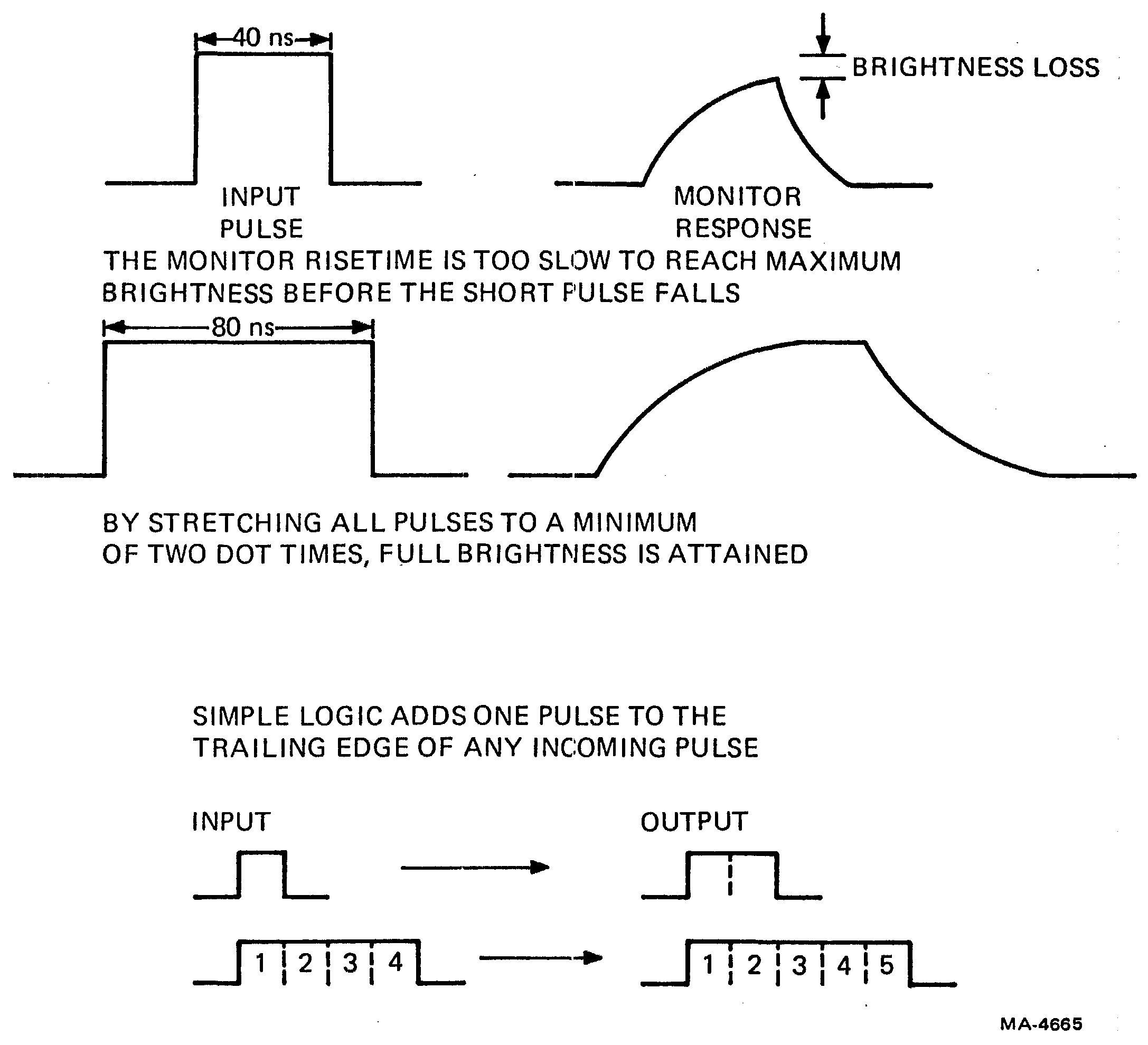
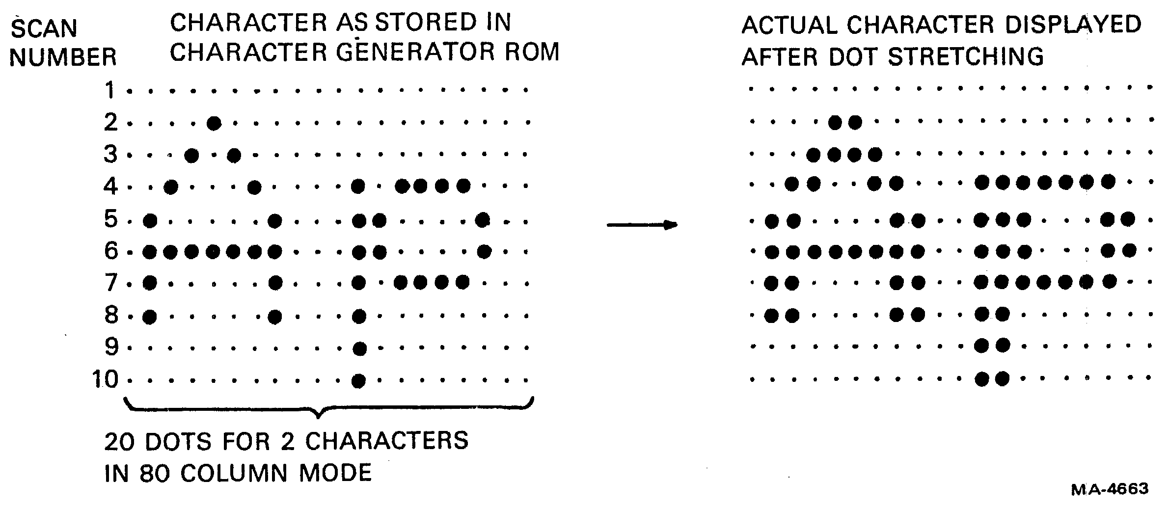
Refer to the print set and to Figure 4-6-20. The address counter (E21, E22, E25, E30) is three presettable 4-bit binary counters cascaded to form 12 bits with an additional flip-flop that provides a 13th bit of address to the screen RAM. Vertical reset clears the counter to an initial hardwired value of 2000H so that the video processor always begins to process from that location after a vertical reset. The counter is loaded with a new address at the end of each DMA when the address load signal appears. The counter counts forward from this address at the character clock rate, using the address count (ADDR CNT H) signal. ADDR CNT H only occurs during Hold Request; thus, the counter only counts during the DMA portion of each line. The address is loaded at the end of the DMA scan and held until the next DMA begins. The 13th bit is programmed by D4 in the high byte of a DMA address. The VT100 firmware programs this bit high to access address 2000H plus the contents of the 12-bit counter. But if D4 were programmed low DMAs would access address 4000H plus the contents of the 12-bit counter.
In double-width mode, the address count pulses occur half as often as in normal width. The line buffer receives the normal number of WRITE LB pulses, however, so each character gets copied into two adjacent locations in the line buffer.
Tristatable latches (E26, E33) store the address counter outputs for a character period to increase the speed of RAM accesses that would otherwise be slowed by the long propagation delay of the counters. They provide sufficient output power to drive the address bus of the basic terminal controller board and the AVO if present. The outputs are disabled during the non-DMA period to prevent conflict with the microprocessor address bus.
Data arrives at the screen RAM latch (E20) during a DMA cycle and is latched in by the character clock. During the DMA the tristate buffer (E15) is enabled. Data passes through it to the line buffer (E11, E17) for storage and to the character generator latch input (E16). The line buffer is a 256 × 8 RAM that can hold one full line of data including the three end bytes. The line buffer is written when WRITE LB L is asserted in the middle of each character clock period. Its outputs are disabled during the DMA by the Hold Request signal. During non-DMA operation, the screen RAM latch samples the 8080 data bus at the character rate but the tristate buffer is off so the 8080 data has no effect. However, the outputs of the line buffer are enabled and the same data is presented to the character generator latch as was presented during the previous DMA scan. The address signals for the line buffer are described in Section 4.6.2.7.
The character generator is a ROM that is addressed by the coded representations of the desired characters stored in the screen RAM. Each code is used as the high 7 bits of the address to a 2K × 8 ROM (that provides enough storage for 128 characters). (The eighth character bit is the base attribute input to the DC012.) The low four address bits are provided by the scan counter in the DC012. The seven character bits combine with the 4-bit scan count from the DC012 to give an 11-bit address to the ROM. The data stored at each (scan + character) address are 8 bits representing the presence or absence of dots of light at sequential horizontal positions within that scan. Figure 4-6-18 shows the patterns supplied in the standard VT100 character generator ROM.
If the alternate character generator ROM and the advanced video option are present, the AVO may assert ALT CHAR SET L to disable ROM E4 and enable ROM E9 when the alternate character set attribute is set.
If the AVO is installed without the alternate character ROM, any character cell in which the alternate set is selected will appear white (black if reverse video). See Appendix A (SCS) for selection of alternate characters.
If it is necessary to use a different main character set than the one provided in the VT100, but an alternate character set is not required, the following arrangement may be used.
To use a UV erasable PROM in the socket for E9 (which must have Intel 2716 pinouts), cut jumper W4 and insert jumper W5 to put +5 volts on pin 21. Only later VT100s have these jumpers. The access time of the ROM must be less than 300 ns to guarantee operation in 132 column mode.
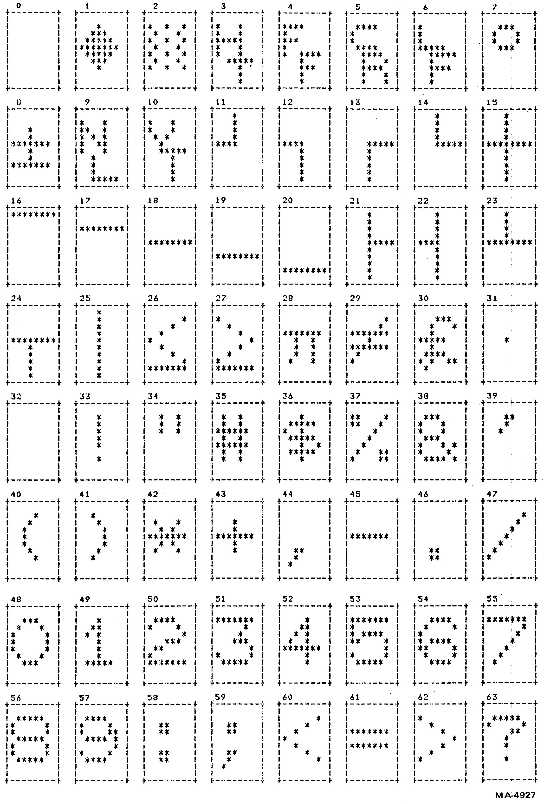
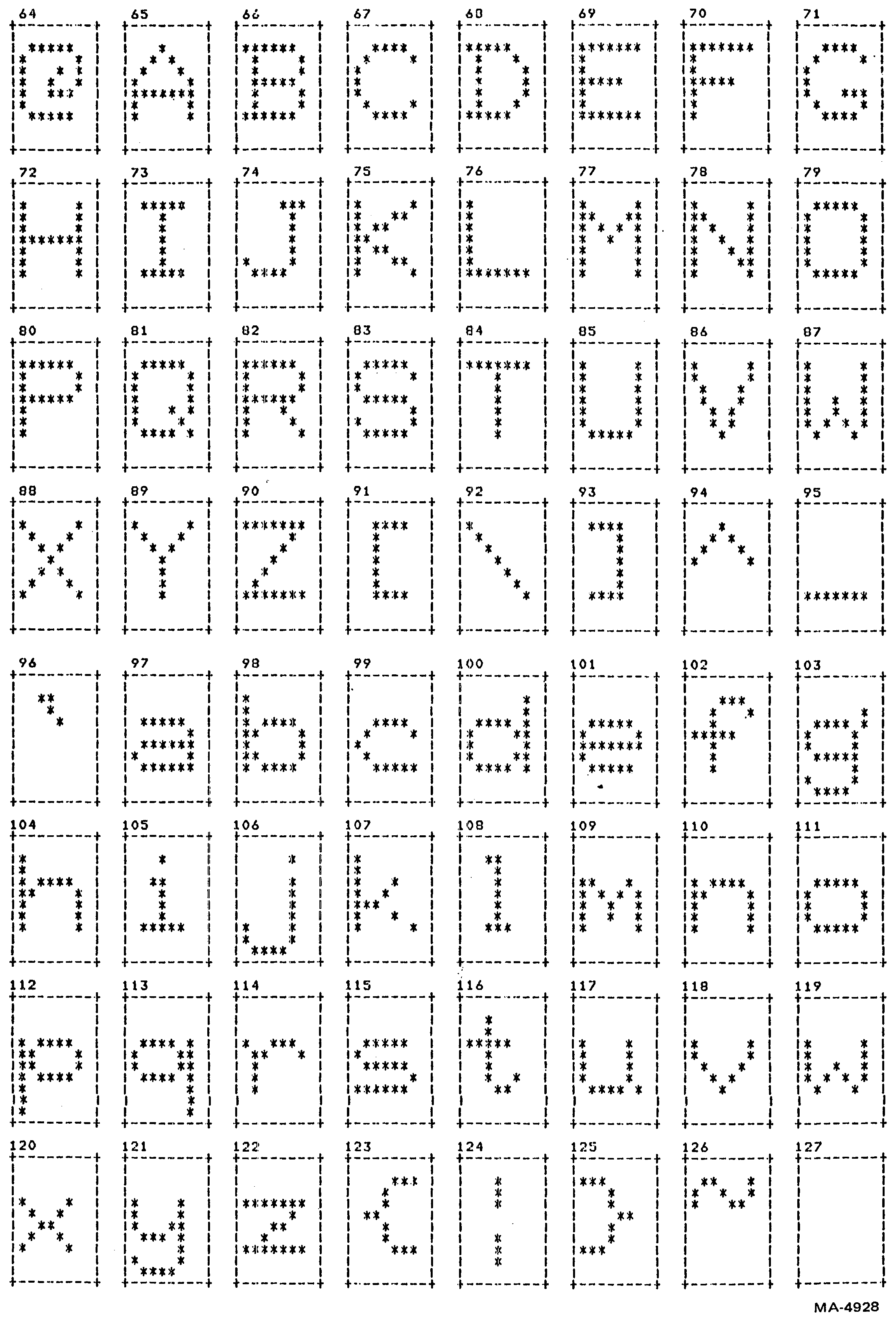
When VSR LD H is asserted, seven of the eight output bits from the character generator ROM are latched into the shift register and one is latched into a flip-flop (Figure 4-6-4). At the same time, the last bit shifted out by the video shift register (VSR) during the previous character time is latched into the first bit position in the VSR. The VSR is continuously clocked by the dot clock. The first bit shifted out in the new character time is the same value as the last bit of the previous character, providing horizontal continuity of characters from one character cell to the next. The seven new bits are then shifted out.
Meanwhile, the flip-flop that stored the eighth bit has delivered that bit to the serial input of the shift register. This bit was shifted into each successive register position as the first eight bits were shifted out. Now the shifting continues, for one more bit in 132 mode, and for two more bits in 80 mode, causing the last bits shifted out to be the value that was stored in the flip-flop.
VSR LD H then latches the next character into the VSR and flip-flop, with that last, multiply-shifted bit in the first position. In this way, one bit from the character ROM defines the two or three dots between characters, while seven bits define the character itself.
At the end of the scan, horizontal blanking forces the flip-flop output low. Since blanking lasts more than one character time, the low level will be shifted to the first position before the start of the next line. This ensures that the first dot on the next scan will be at the screen background level.
The 7 bits of each character address in a line go to an 8-input terminator detector gate as they are passed to the character generator ROM. Only seven bits are examined because the eighth bit is an attribute and does not contribute to the uniqueness of a character. The last bytes in each line are a terminator character and two address bytes. Only the terminator character activates the gate. During the character time when the terminator reaches the detector gate, the first address byte is at the input to the character generator latch and the second address byte is at the input to the screen RAM latch. On the next character clock, the terminator causes the DC012 to blank the display and end the Hold Request. The latch outputs now contain the two address bytes. The low order byte is at the inputs to counters E30 and E25, while the low four bits of the high byte are at E21. The fifth bit is at the input to flip-flop E22. This bit is normally high; it allows future development of screen RAM size. The high three bits go to the line attribute inputs to the DC012.
The address load (ADDR LD L) pulse, timed to arrive before the next character clock after the terminator, loads the address counters, flip-flop, and DC012 inputs with the two final bytes. The counters and flip-flop designate the address of the first character of the next line to be displayed.
Figure 4-6-19 shows the complex timing in the video processor during the first scan of each new line of characters. The entire scan is shown, with the rep,eating portion compressed into the area represented by dashed lines. The diagram is for 80 columns, single width display as the VT100 is currently programmed. Diagrams in the DC011 timing chip description (Section 4.6.2) show the differences in signals in other modes.
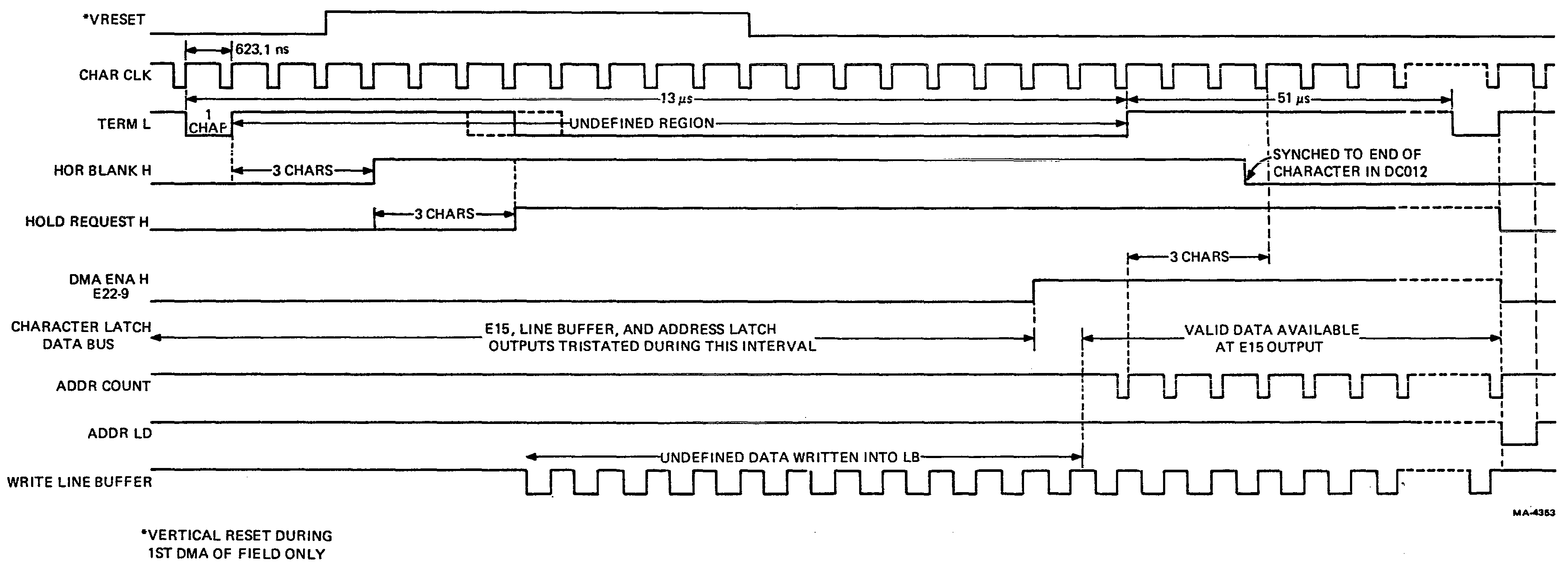
The first line shows the Character Clock. This continuous signal is the time reference for all DMA events.
The terminator occurs at the end of the previous scan. TERM L goes low for one character clock and then goes to an unspecified state which depends on the random characters that appear at the terminator detector gate. Character Clock continues to shift data through the character latches but invalid data are present in the character latches and stored in the line buffer until just after DMA ENA is asserted. The terminator forces the video output to black or white (depending on normal or reverse screen) effectively blanking the end of the line (Section 4.6.11). It also ends any DMA process in progress. The terminator’s blanking effect is taken over by Horizontal Blank, and the terminate flip-flop in the DC012 is held cleared until just before the first character in the next scan. This prevents undefined data from triggering the flip-flop and blanking the whole scan.
Horizontal Blank occurs 3 characters after Terminate in 80 column mode and 5 characters after in 132 column mode. It forces all video to black (regardless of normal or reverse screen) for the horizontal retrace interval. The Horizontal Blank signal, as an output from the DC011, ends one-half character before the video actually needs to unblank. This early transition releases the clear for the terminate flip-flop in the DC012. The blank signal is resynchronized to Character Clock in the DC012.
Hold Request silences the microprocessor so that the video processor can DMA data out of the screen RAM. It is initiated when the scan counter in use is equal to 0, or at the setting of the new scroll zone flip-flop. The terminate flip-flop must be cleared for Hold Request to occur. The start of Hold Request is delayed by three character times from Horizontal Blank to allow the counter in use to settle before the 0-boundary is detected. Hold Request is ended by the detection of terminate at the end of a DMA scan.
DMA Enable is generated from Hold Request and the microprocessor’s hold acknowledge (HLDA) by discrete logic on the board (E22). It is enabled by the first rising edge of LBA4 if HLDA from the 8080 is available. This ensures that the 8080 has given up the bus before DMA ENA H enables the DMA address counters onto the bus and drives MEM R low. DMA ENA H is cleared by the end of HOLD REQUEST H. While the use of LBA4 ensures that enough time has elapsed from the start of HOLD REQUEST H to guarantee that the 8080 is in its hold state, the use of HLDA H on the D input of the DMA Enable flip-flop is required to prevent HOLD REQ from preventing a power-up cycle in the 8080.
The character latch data bus is shown to be tristated from the start of Hold Request until the start of DMA Enable. Then it starts moving data through the video circuits.
Address Count begins three character times before the end of Horizontal Blank (Section 4.6.2.4).
Address Load is triggered by the falling edge of HOLD REQUEST H. It stores the line attributes for the next line and loads the address counters with the pointer address bytes at the end of the DMA line of characters. This address is the location of the first character of the next line to be DMA’d.
Write Line Buffer L is described in Section 4.6.2.3.
Figure 4-6-20 is an expansion of the DMA timing showing the contents of the various storage devices at different times at the beginning of the active display of a scan.
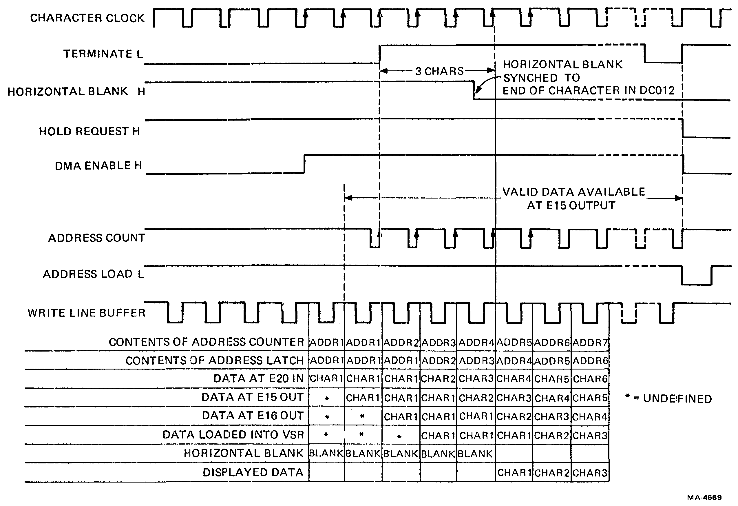
The display is blanked by Horizontal Blank during the horizontal retrace interval, and by Vertical Blank during the vertical retrace interval. These hardware signals ensure that the CRT beam is turned off while it moves backward through the active screen area. Horizontal Blank controls the video signal inside the DC012. Vertical Blank controls the video signal at the video output circuit. Figure 4-6-21 shows a frame of video divided into segments of one horizontal and vertical movement of the electron beam over the CRT face with respect to time. Figure 4-6-21 plots the screen and its invisible regions by relating the screen area to the state of blanking at any given time. The top-left corner represents the first visible dot position. The terminator position is the place where no data is displayed but Horizontal Blank has not yet taken effect. Horizontal Blank then takes effect all through the horizontal retrace period and unblanks just in time for the first dot of the next scan. After 240 scans, Vertical Blank turns off the beam while the beam returns to the top of the screen.
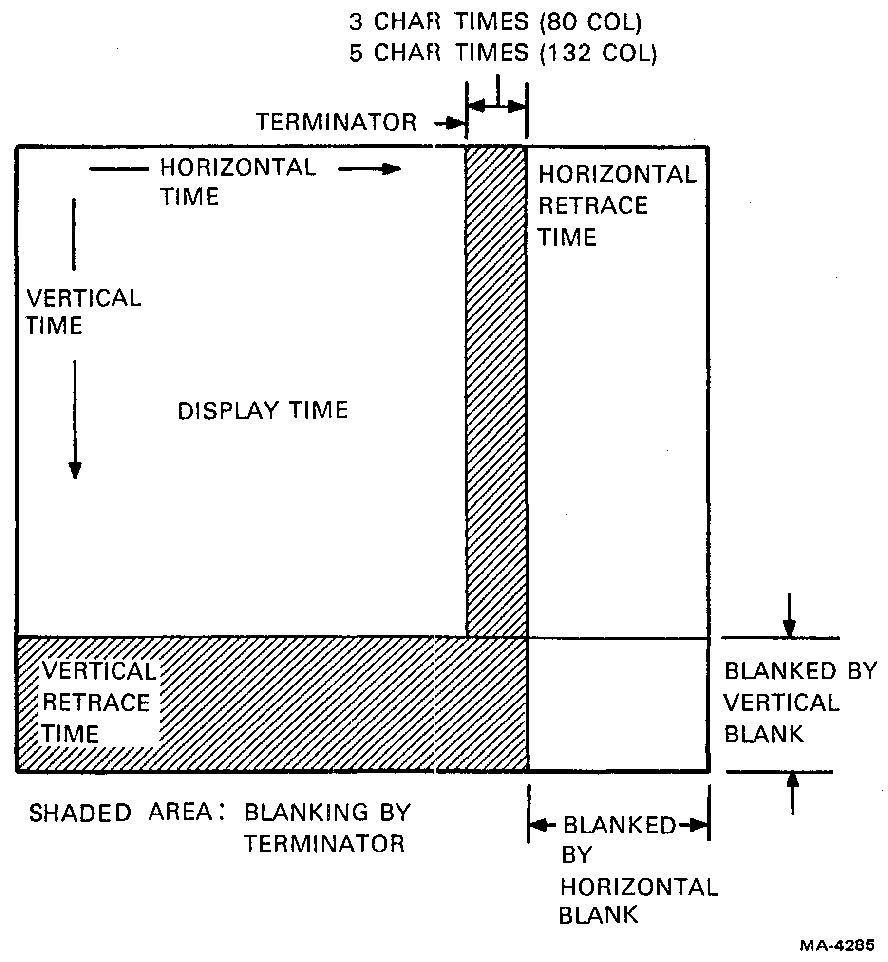
The horizontal blanking signal is timed to provide 83 columns of unblanking in 80 column mode, and 137 columns of unblanking in 132 column mode. The VT100 is currently programmed so that the three or five extra columns are blanked by Terminate. In normal screen mode, this termination forces the beam to black, but in reverse screen, termination forces the beam to the screen background intensity. This means that in reverse screen mode, the last character that can fit on the screen is three or five characters in from the right edge of the illuminated screen. Because hardware blanking allows 83 or 137 columns on the screen, future program developments may allow the microprocessor to format the screen RAM for this ability. The main adjustment is to the position of the terminator and address bytes relative to the starting location of the line. Terminate, as the first character in the line, creates short lines during the vertical blanking interval to conserve memory while maintaining synchronization of the line address system.
Refer to the print set for the circuits discussed in the next three sections.
The two video outputs from the DC012, Video Out 1 and Video Out 2, are combined with Vertical Blank in two open collector nand gates (E7). The outputs of the open collector gates are wire-ANDed with Graphic 1 and 2 IN (E29) from any option board that may be present. The combined outputs of E7 and E29 pass through and either float the base of Q4 to +12 V through R38, R39, and R36 or R37, or pull Q4’s base down to some value determined by one, the other, or both resistors R36 and R37 in parallel. These four conditions represent the four levels of intensity visible on the screen: black, dim, normal, and bright.
The combined outputs of E7 and E29 control the voltage at Q2’s base through R31, R32, and R33 in the same manner as described above. At the same time, composite sync controls Q2’s base through R33 and R30. The result is a 75 ohm output from the terminal controller consisting of four intensity levels (including black) and composite sync. This signal can directly drive a standard video monitor or sync can be extracted to synchronize an external device for input to the terminal. The output is dc coupled. Although the use of dc coupling is not in strict agreement with EIA specification RS-170, this presents no problem with most monitors because they are usually ac coupled. See Figure 3-4 for an illustration of the composite video output.
The video input stage terminates a standard video signal in 75 ohms. R43 and D7 bias Q5 into linear operation, while C16 passes video around the bias network. R44 suppresses oscillation in the stage and D6 protects the transistor from a reversed polarity input. D5 biases the base of Q3 and R41 is the load resistor for the amplifier. R42 stabilizes the amplifier by emitter feedback. The video input affects only the picture on the internal monitor as described below; it does not appear at the Composite Video output.
The video input and output circuits can produce: a range of voltages (as compared with circuits that can produce only two values, white or black levels for example). To do this they are biased into linear operating conditions. High current biasing provides the necessary high speed operation. Because of the high power dissipation that results, the video circuits use discrete transistors.
Direct Drive Video is the output from the terminal controller to the video monitor’s cathode driver transistor. It is a combination of Video Out 1 and 2 signals from the video processor, and by means of a parallel transistor Q3, the signal from the video input (labelled Graphics Video In on schematic sheet BV4). The monitor already receives horizontal and vertical deflection signals directly from the terminal controller, so the terminal’s video input only requires picture information. If the blanking level on the video input is greater than zero volts, the screen background intensity cannot be black. Note that composite sync on the input is also ignored by the terminal controller, because the terminal’s timing is produced entirely by a crystal and cannot be synchronized to external signals. As explained in Chapter 3, external sources may be synchronized with the composite sync signal that appears at the output jack.
Q3 and Q4, in parallel, are one amplifier with common emitter and collector resistors. The emitter feedback resistor is R40, connected to +12 volts. The collector load is the input impedance of the monitor to ground in parallel with R54 and anyone of 32 parallel combinations of R49, 50, 51, 52, and 53. This arrangement allows either transistor to set the minimum current through the collector and emitter resistors with the voltage that appears on its base. The other transistor then cannot reduce the current by being turned off. It can increase the current, however, if it receives a larger base voltage. Thus the output is always proportional to the greater of the two inputs. Two identical input signals do not add up because of the common emitter resistor. If the voltage on Q3’s base is more positive than the voltage on Q4’s base, a voltage at the base of Q4 causes a 0.6 volt different voltage at R40 (both emitters), and current to maintain that value will flow through Q4 and R40 (as well as the collector load). If the same voltage as at Q4’s base is applied to Q3’s base, the voltage at the emitters will not change due to the identical voltage drops across the two base-emitter junctions. There is no current change and so the output remains constant. D8 and R48 provide an extra 0.6 volts of bias for the cathode drive transistor in the monitor. C17 bypasses the diode for video signals.
The 32 combinations of resistors in the collector load of the output stage are produced by connecting any of the selected resistors to ground through an open-collector buffer. The buffer inputs come from the D/A (digital to analog) latch. This latch is written into as an I/O device by the microprocessor. In SET-UP mode, the microprocessor uses the up and down cursor keys as inputs to a 5-bit software up-down counter. At each vertical reset, the microprocessor writes the current contents of the counter into the latch. Thus there are 32 possible intensity levels available, controlled from the keyboard, and frequently updated to minimize the effects of soft errors. Note that the variable intensity only applies to the internal monitor.
The microprocessor communicates with the video processor in the following ways.
This section describes the processes of control through the screen RAM and scrolling. The meaning and mechanism of the line and character attribute bits and the DMA process are discussed in the video processor section. The setup process is discussed in the 8080 section.
Three bytes of control data are located at the end of each line of characters (Figures 4-7-1 and 4-7-2). The first byte, called the terminator, is 7FH and is a unique character that the video processor recognizes as the end of the line. (The high bit is not tested by the terminator gate but is set to zero to avoid complications in the attribute circuits.) Five bits of the next byte and all of the last byte are an address pointing to the first character of the next line to be displayed. The three remaining bits in the first byte define the line attributes of the line pointed to by the address. The high bits of the address are hardwired at the address latch so that when vertical reset clears the address counter, it will point to the ROM-RAM boundary at 2000H.
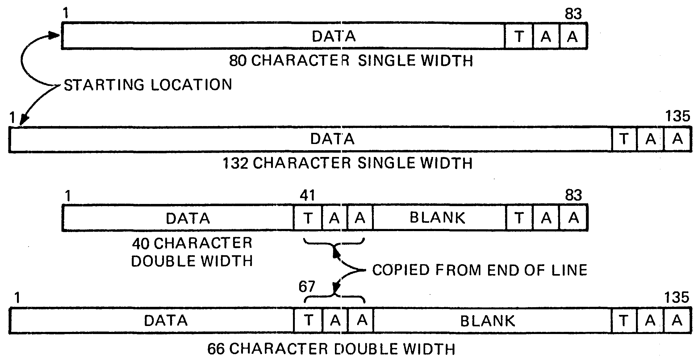
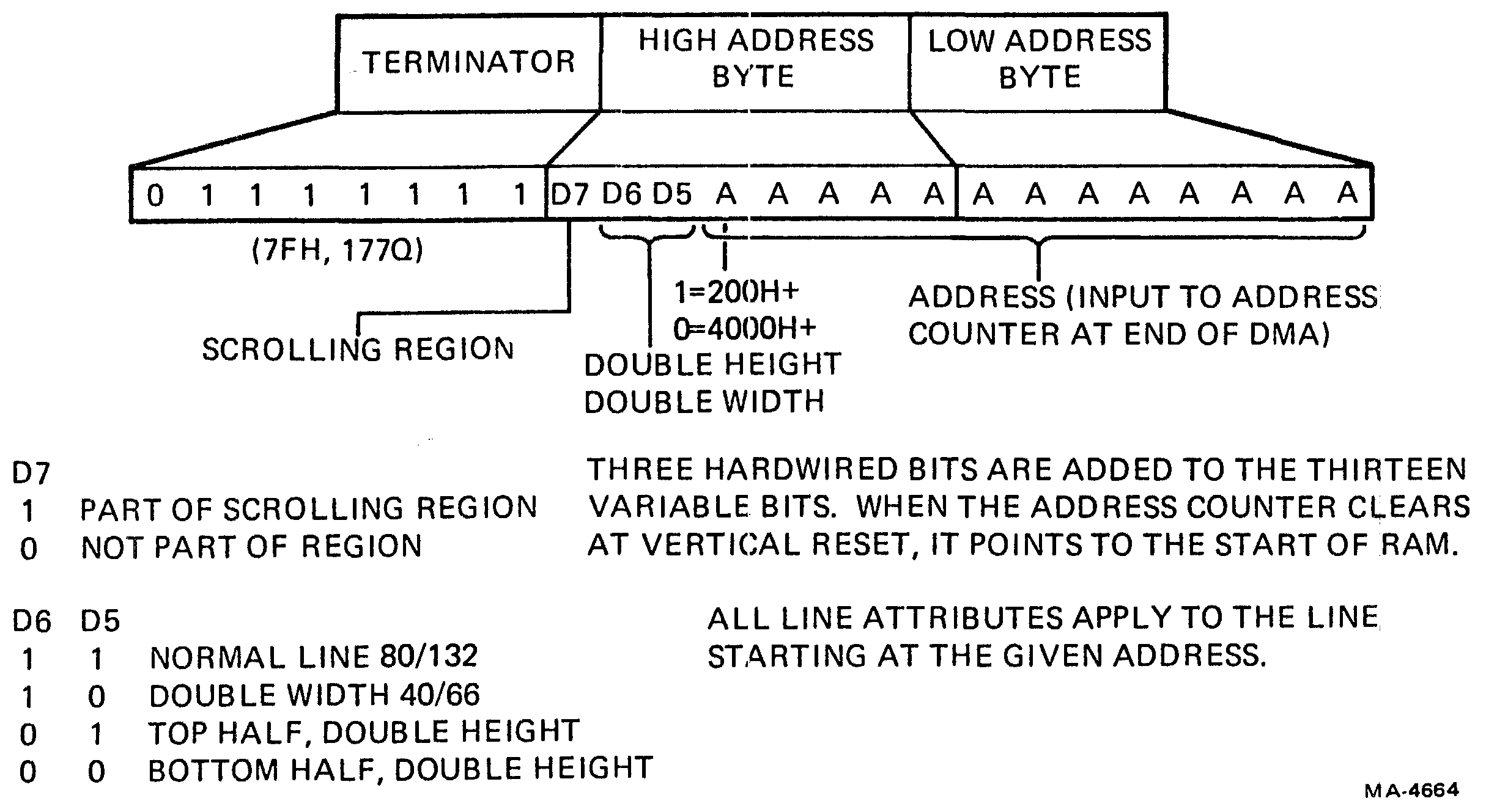
During power-up or reset the microprocessor writes terminators and addresses into the screen RAM according to the specified line length and refresh rate. The 50/60 Hz refresh choice causes the microprocessor to arrange fill lines to place the beginning of the display in the right time slot relative to the vertical reset and vertical blanking signals. The line length determines the locations of the control bytes. For 80 column lines, the memory space is arranged in 83 byte intervals; for 132 columns, the interval is 135.
The memory organization for 80 column, 60 Hz mode is shown in Figure 4-7-3. Location 2000H is the start of the RAM space. When Vertical Reset resets the DMA address counter in the video processor to zero, the counter latch points to this location. The first 18 bytes are fill lines. Byte 2 is the only one written differently when 50 Hz refresh is selected. The change causes a longer fill time during the longer vertical blanking interval.
About 700 bytes of RAM are reserved for the microprocessor stack, scratch pad, and setup areas. The rest of the 3K RAM is devoted to screen information. At program start, the microprocessor reads the contents of the NVR into the setup area (Section 4.7.11). Then the microprocessor reads the setup parameters, erases the screen area and writes in terminator and address/attribute bytes at the selected line length intervals. The address at the end of each line points to the first location of the next line. At start-up, this is the next physical location. The end of the last line points to a fill line which points to itself. The fill line repeats until vertical reset.
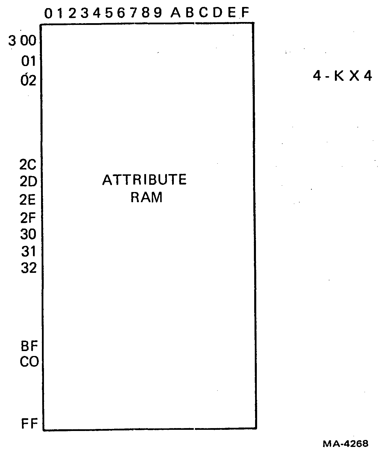
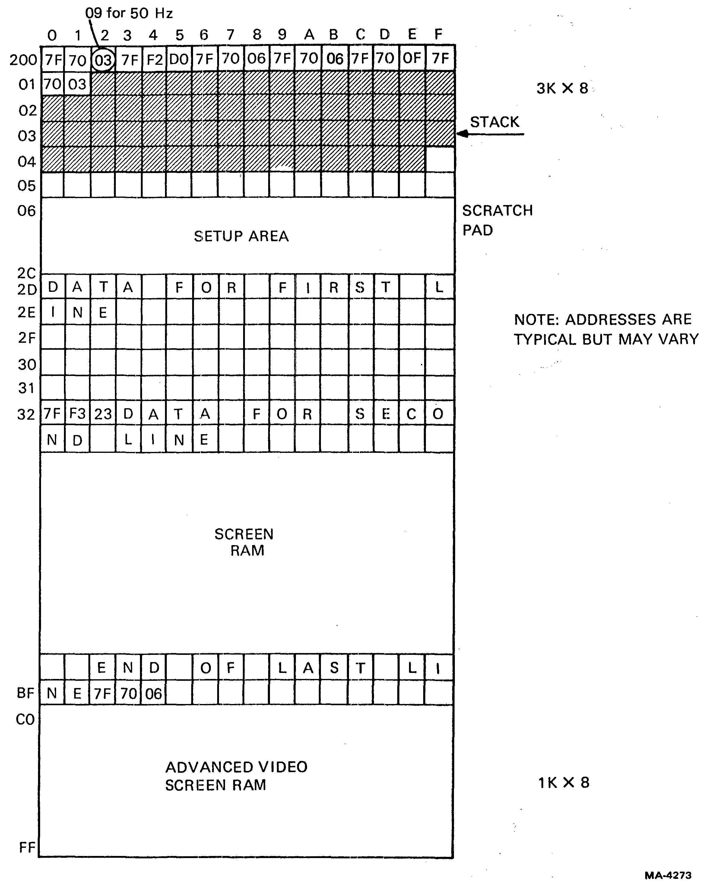
The video processor clock is constant so it always takes the same amount of time to refresh the screen. At any refresh rate there are some fill lines needed at the beginning of the frame so the data can be displayed starting a few lines down from the top edge of the picture tube. At the slower refresh rate, the video processor must idle for awhile between frames. Figure 4-7-4 illustrates the vertical position of the electron beam in the CRT as a function of time for the two refresh rates. The beam sweeps down the display area at the same rate for both refresh rates but because 50 Hz has a longer interval between sweeps, the beam travels farther off the ends of the display. While the beam is off screen, fill lines maintain synchronization in the video processor address system. More fill lines are needed at the top and bottom of a 50 Hz screen than a 60 Hz screen. Figures 4-7-5 and 4-7-6 show the top-of-screen fill line operation for both refresh rates. Starting at location 2000H, the terminator-address triplets point successively to one another and then to the first displayable line of data in the screen RAM. The change of one byte in the group changes the fill line delay from two lines for the 60 Hz refresh rate to five lines for the 50 Hz refresh rate. Figure 4-7-7 shows how the single bottom fill line repeats itself as many times as needed until vertical reset stops it and clears the address counter to 2000H.
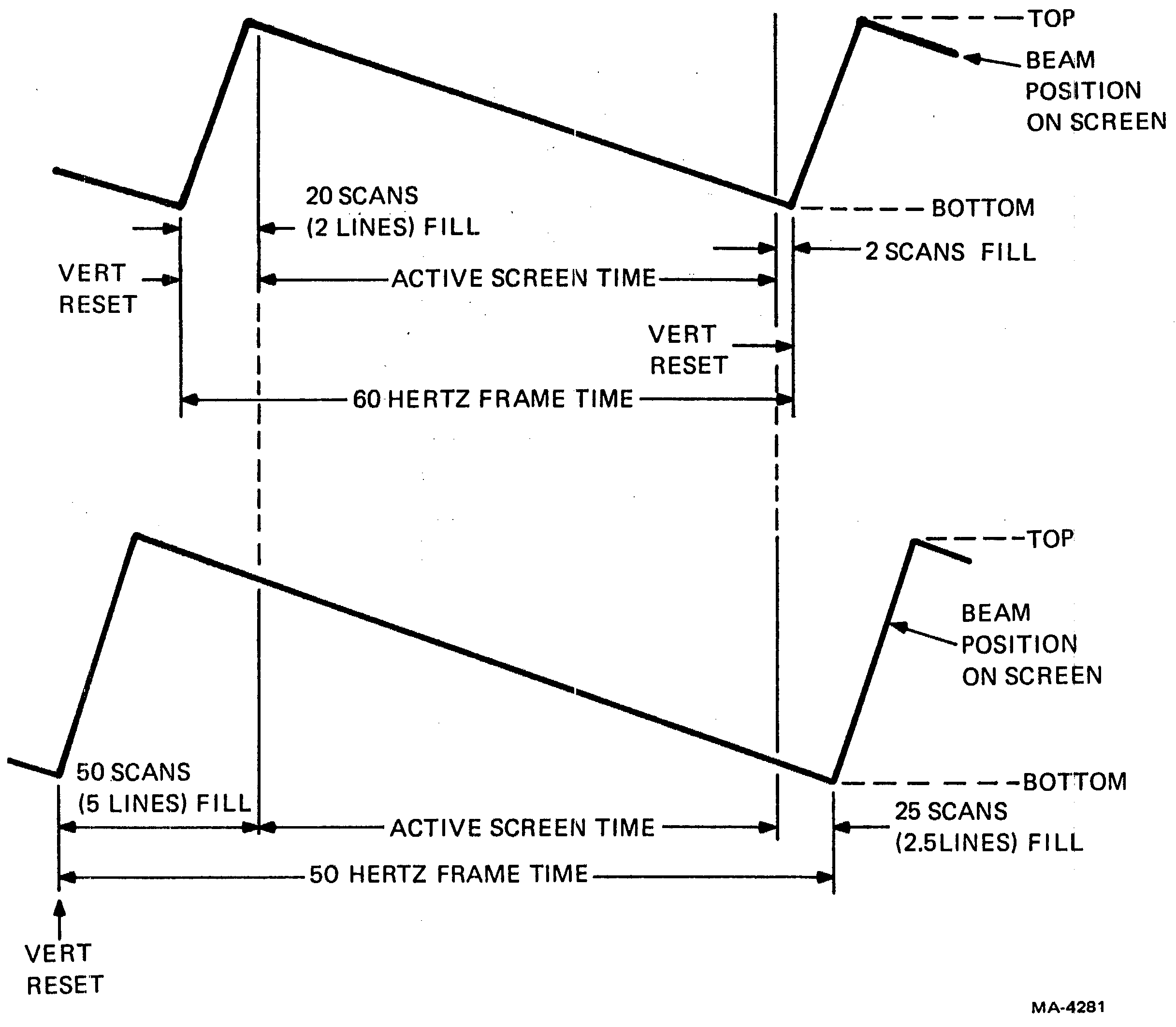
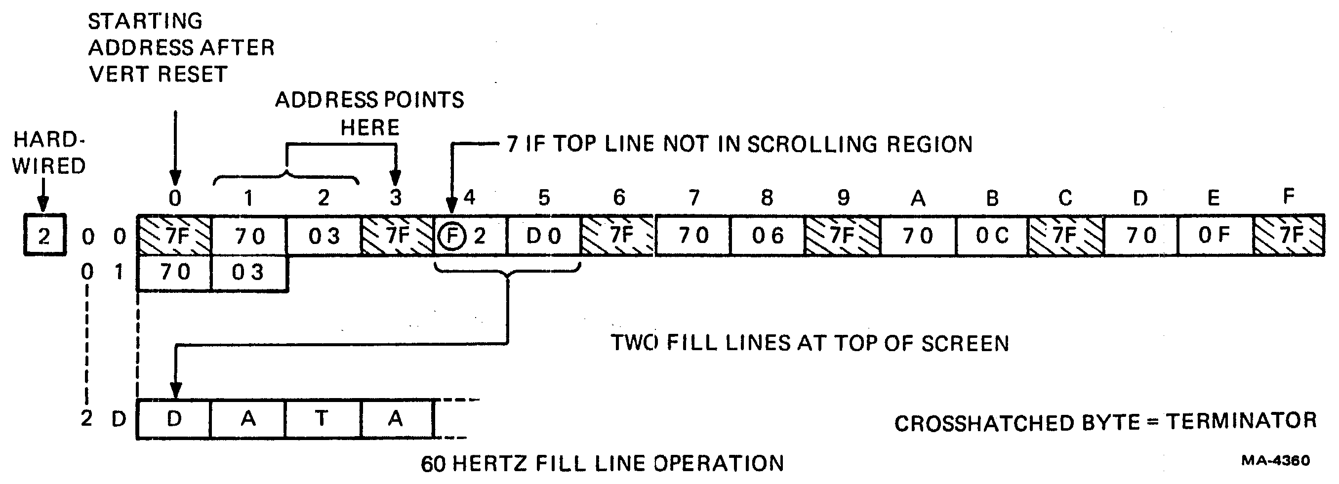
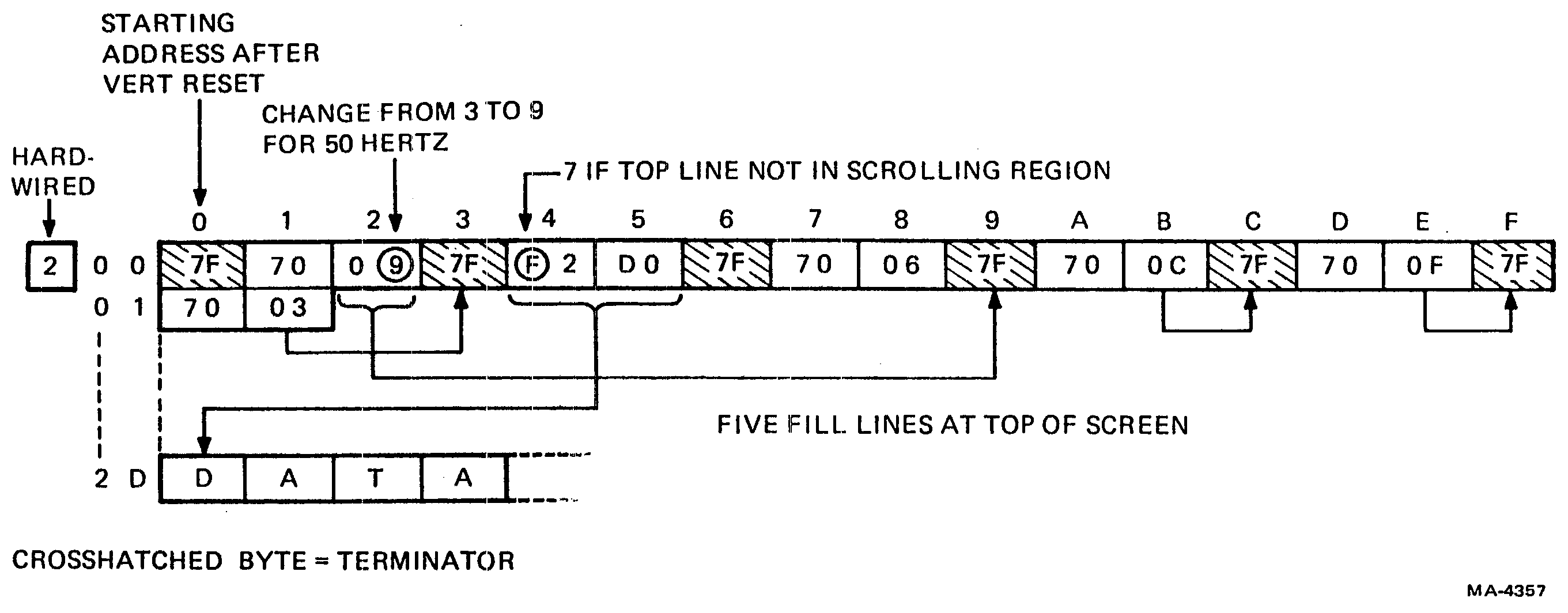
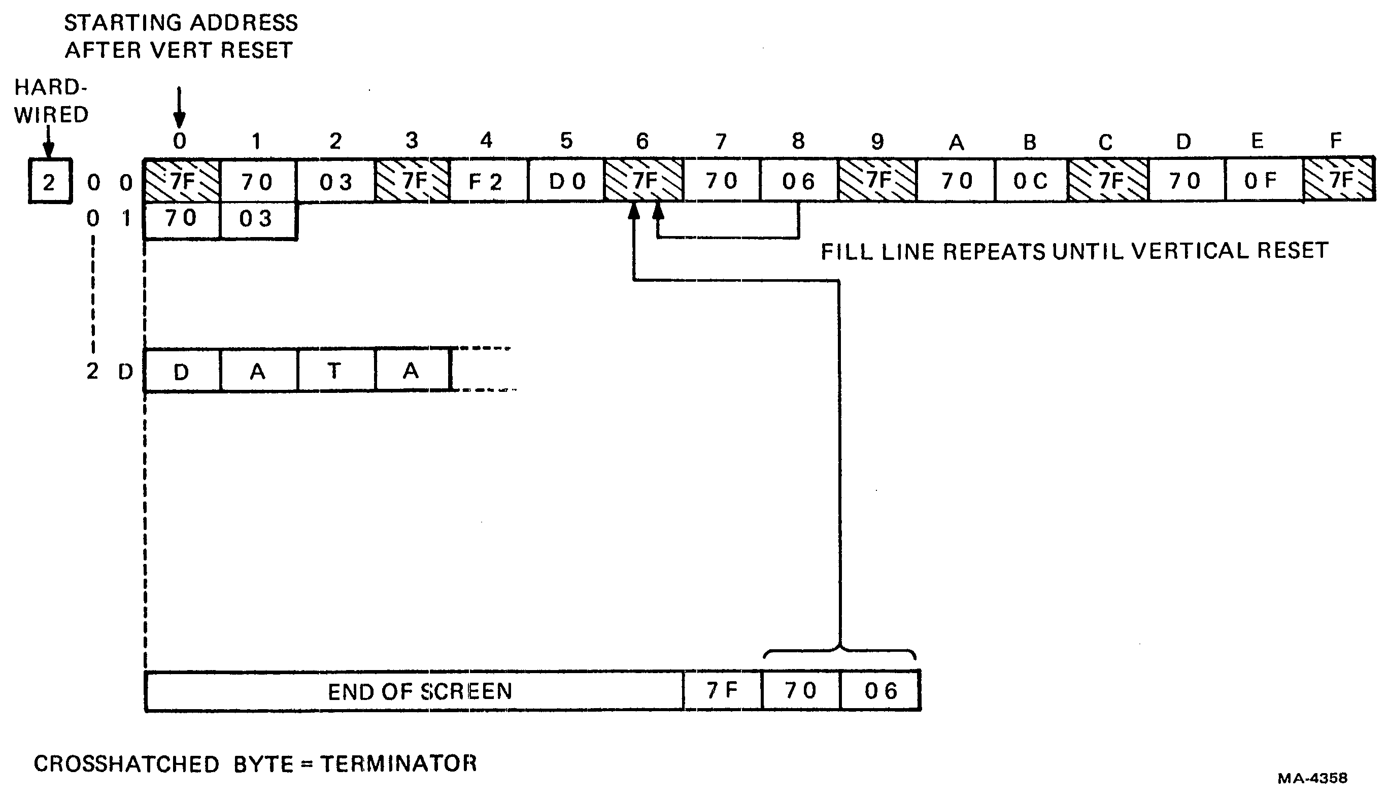
In 132 column mode 25 lines are set up in the RAM for a 24 line screen, and 15 lines are set up for a 14 line screen. With the advanced video option, 25 lines are set up for either 80 or 132 column lines. Except during a smooth scroll, only 24 lines are seen. But the microprocessor keeps the 25th line erased in reserve, and when a scroll takes place, the 25th line becomes visible as the new top or bottom line (depending on scroll direction). All new characters after the command that caused the scroll go into this line. In preparation for a full screen scroll up, the microprocessor writes the address of the repeating fill line into the 25th line pointer as well as the 24th line pointer. This saves processing time during the address rearranging which is a part of each scroll.
The line organization changes when the first scroll occurs. Pointer addresses are revised any time a line is added to or removed from the screen. The extra line is used whenever the screen needs to be scrolled up or down. Then the extra line is displayed and the old top or bottom line is scrolled off screen, erased, and made available as the new 25th line.
To understand the pattern of address changes, consider the display to consist of two parallel entities: a physical screen and a logical screen.
The physical screen is the memory organization already described. The key feature of the physical screen is the pointer address, contained in each line, that causes the hardware to chain the lines into a sequence for display. After a series of split screen scrolls, the physical screen will contain some arbitrary sequence of line addresses.
For example, if the original order of lines was 1,2,3,…23,24, the new order might be 16,13,24,…1,8. With only this organization, a command to insert a line at the fifth position on the screen would require the microprocessor to follow the various pointers around the RAM until it reached the fourth such pointer in order to learn where the physical address of the current fifth line was in the RAM. Instead, a list of locations is maintained in the logical screen.
The logical screen is a 25-entry table that points the microprocessor to the proper locations for shuffling (rearranging) line addresses and placing the cursor in the screen RAM. The table is set up in a contiguous area of memory starting at the location named LATOFS (Line Address Offset Table). Figure 4-7-8 shows LATOFS after at least one split screen scroll and in the process of another split screen scroll. Each entry in LATOFS is the number of a line in the physical screen. The position of an entry in LATOFS refers to the position of a line on the screen. The microprocessor updates LATOFS just before each scroll so that the microprocessor can rewrite line addresses during the vertical interval. The microprocessor reads the table to learn which line in RAM is available for writing as the new 25th line or which line is being used at a given position on the screen. For example, to insert a character in the fifth line, if the fifth entry in LATOFS is “20,” the microprocessor calculates the starting address of the 20th physical line in RAM. The character address can be calculated from that starting address and the cursor position within the line.
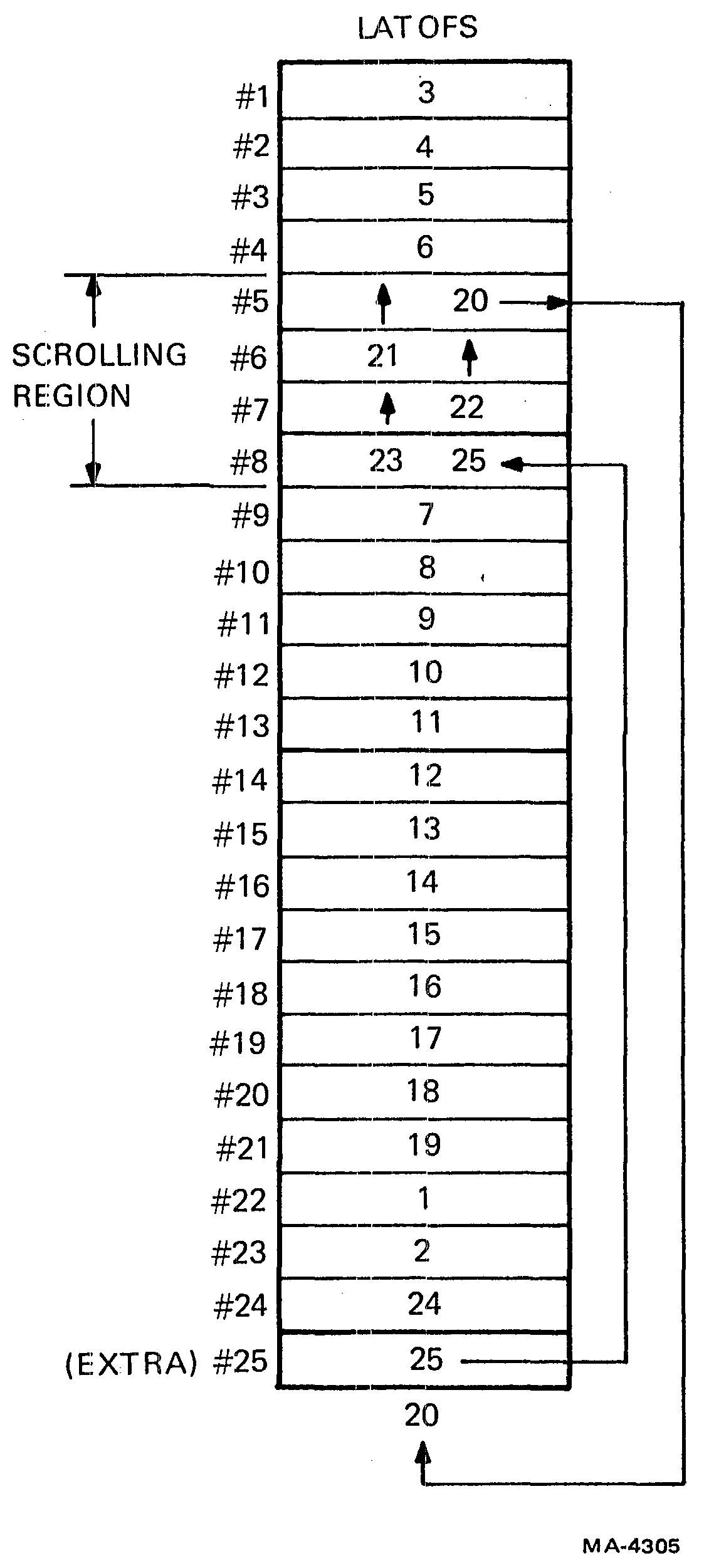
Consider the case of a full screen upward jump scroll. The line in LATOFS #25 is the extra line, not seen except during smooth scrolls. When a line is jump-scrolled off the screen, it becomes the extra line, and the RAM area that was line 25 becomes the new last line. The scrolled-off line is erased and its first location is noted as the starting point for new data entry into the RAM. The physical screen addresses that chain in which the displayed lines must be revised. And since the last fill line must point to the new first line, which formerly was the second line, the revisions must be done before that last fill line is DMA’d into the video processor.
When a line feed is received, four numbers are stored in memory. These are Shuffle Address 1 and 2 (SHUFAD) and Shuffle Data 1 and 2 (SHUFDT). SHUFAD contains the location of the address that must be changed, and SHUFDT contains the new address that will be inserted there. The two sets are for the pointer above the line that will be scrolled off, and for the pointer on the end of the line that will be the new next-to-last line (Figure 4-7-9).
The process of changing the addresses is called shuffling because most of the computation is done in advance. The change is made quickly in a simple point-swap-point-swap sequence. One other item prepared in advance is the pointer on the 25th (to become the new last) line. The pointer on the present last line is copied onto the new line. The shuffling process takes less than 550 microseconds (the time between DMAs). The screen’s apparent jump up or down is entirely the result of the revision of pointer addresses. If, for example, the shuffle occurs during the 15th line, no effect will be visible until the end of the frame, when the extra line is pointed to but is outside the viewable area. After vertical reset, however, the shuffled address at the top of the screen will point to the old second line. The first line is gone, and now there is room on the screen for the extra line and it appears.
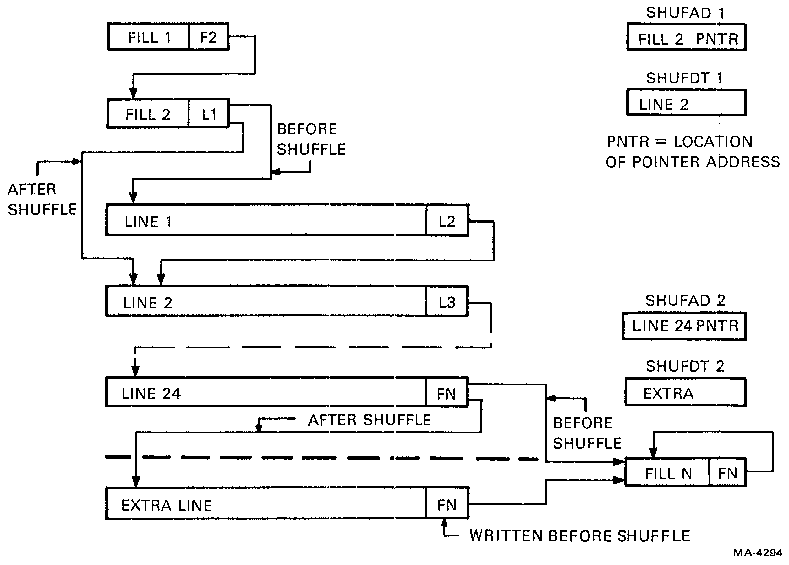
The shuffles for smooth and split screen scrolls must be synchronous with vertical reset to avoid disrupting the appearance of the display. Therefore, only one line feed can be executed during a frame. However, in the case of full screen jump-scrolling, the address shuffle may occur at any time. This increases the rate at which line feeds can be executed and improves the terminal’s throughput.
While full screen jump scrolling may occur at any time relative to vertical reset, the two other kinds of scroll are sensitive to the time when shuffling occurs. If a split screen scroll region (say 10 lines in the middle of the screen) is revised while the display is scanning that region, only the change at the bottom of the region would take effect during that frame. The extra line would appear at the bottom of the region and the following lines on the screen would be pushed down one line from their locations in the previous and succeeding frames. The appearance would be that of a flash of mixed-up data below the scrolling region. Therefore, all changes are made during the vertical interval, ensuring that the proper number of lines is consistently displayed because the video processor cannot ever attempt to execute only part of a shuffle sequence.
Logically the screen still flashes in full screen scrolling, but because the extra last line is displayed beyond the end of the screen, Vertical Blank blanks the display. The shuffle is a two part process, with the two address bytes transferred in separate operations. If the shuffle is not complete before the DMA that accesses the shuffled address starts, the address that gets read may not be valid, and garbage may be displayed thereafter. The random start of the shuffle process relative to the video processor’s DMA timing causes this error.
A scrolling region may be established on the screen, on a horizontal line basis, within which data may be inserted or lines scrolled without affecting the positions of data outside the region. Only one region may be defined at a time, but it may be repeatedly redefined. Full screen scrolling is a special case in which the region margins and the screen margins are the same. A control sequence defines the region by specifying the line numbers of the top and bottom of the region. When the control sequence arrives, the microprocessor stops taking characters from the silo and waits for the current scroll to end. It then checks the parameters for legality (top less than bottom, bottom less than 14 or 24). If they are bad, the sequence is ignored and the next character is taken from the silo. If they are good, they are stored in locations labelled Top and Bottom. Then starting at the pointer address on the last fill line, the microprocessor sets the fill line’s scroll attribute bit to scroll or no scroll (depending on the specification for top margin) and jumps to the end of the addressed line, setting its scroll attribute bit. The microprocessor continues down through the screen RAM until it reaches the point to line #Top, the line that will be at the top of the scrolling region. It sets the attribute bit there to scroll. Jumping down through the region, the microprocessor continues setting line attributes to scroll until it reaches line #Bottom, the bottom line in the scrolling region. From there to the end of the screen it sets the bit to no scroll.
When a line feed is received, during the remainder of the current frame the microprocessor rotates LATOFS and prepares for the shuffle. The line number at LATOFS #25 (25 in Figure 4-7-8) moves up to the bottom position in the scrolling region (LATOFS #8). The line at LATOFS #5 (20) moves to LATOFS #25, and all the other lines in the scrolling region of LATOFS are moved up one position. The shuffle buffers are set up. (See Figure 4-7-10.) SHUFAD 1 contains the location of the pointer address at the end of the last line before the scrolling region and SHUFDT 1 contains the pointer address for the new first scrolling region line. SHUFAD 2 contains the location of the pointer address at the end of the new last scrolling region line and SHUFDT 2 contains the pointer address for the first line after the scrolling region.
While the LATOFS and shuffle preparations are underway, data may be coming into the terminal. Data received after the line feed stay in the silo until the LATOFS rotation is completed. Just before rotation, LATOFS 25 points to the number of the next RAM line that data should go to. The microprocessor records that location and then performs the rotation and shuffle preparation. Then it resumes writing the data into the line previously noted. When vertical interrupt occurs, the shuffle is performed and the new line is displayed. If no new line feed is received, data will continue to be written into the same line.
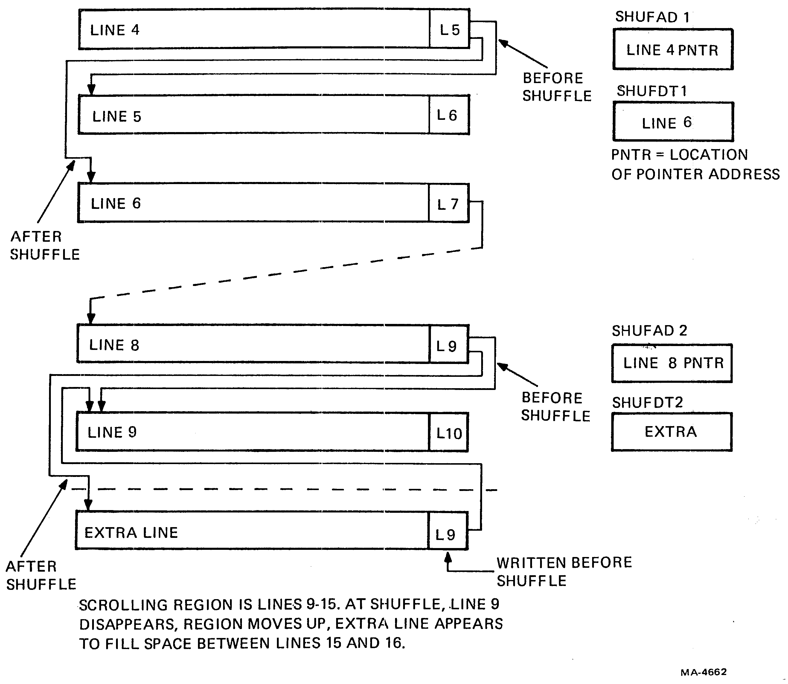
Become familiar with the operation of the scan counter as described in the video processor section (4.6.3.3) before studying this description.
In smooth scroll operation, the VT100 changes the positions of the lines on the screen slowly, so the eye can follow and read the data as it goes by. Instead of moving one character height or 10 scan lines in a single frame, the data moves up or down one scan line in each frame. The smooth scroll rate is thus 6 lines per second at 60 Hz frame rate. Operation is the same for full or split screen smooth scroll. For any given line feed, the effect on the screen is delayed by two frames. Line feeds may queue up so that scrolling is continuous.
Smooth scroll is enabled by a bit in the setup memory that causes the microprocessor to perform all scrolls as smooth scrolls. Whenever a line’s scroll attribute bit is set, it receives its scan count from the offset counter. At vertical reset, the scan counter, used for nonscrolling lines, always resets to zero, but the offset counter is loaded with the contents of the scroll latch. The microprocessor loads the scroll latch with an offset value. If a jump scroll is involved, the offset is always zero. If a smooth scroll is involved, the microprocessor loads an offset value according to the number of frames that have passed since the line began moving.
When a line feed is received the microprocessor waits for the current scroll to end. It sets an internal scroll-pending flag. Then, at the next vertical interrupt, during the frame before scrolling begins, the shuffling process makes its preparations but only to add the 25th line to the display. During smooth scrolling, all the lines will be visible together. The microprocessor, which keeps count of the number of frames in the scroll, loads the scroll latch in the DC012 with an offset value of one. Then, when the second vertical interrupt occurs, the microprocessor performs the address shuffle, the offset counter receives the 1 from the scroll latch, and the microprocessor loads the scroll latch with 2. As the frame begins, the character generator ROM, driven by the offset counter, displays its second scan row on the top line of the scrolling region. The rest of the scrolling region is moved up by the same amount, so the last scan in the scrolling region is the top scan of the 25th line.
Succeeding frames contain the data moved up scan by scan as the microprocessor loads the scroll latch with larger offset values each time. During the ninth such frame, only one scan from the top line and nine scans of the bottom line are visible. The microprocessor loads 0 into the scroll latch. If the microprocessor made no other change, then on the next frame, the data which had been moving slowly up would jump back down to its original position. Therefore, another address shuffle is performed at vertical reset. The top line of the scroll region is discarded and the 0 offset applies to the former second line. The old top line is erased and becomes the new 25th line that will appear in the next scroll.
In a split screen smooth scroll, the scan count to the character generator ROM must switch between the normal scan counter and the offset counter. (Please remember that full screen scroll is a special case scrolling region, and that jump scrolling is a special case offset count of 0.) The scrolling attribute bits, which were set when the control sequence that defined the region arrived, operate the counter multiplexer (MUX).
Refer to Figure 4-7-11 and suppose that the smooth scrolling region extends from line 5 to line 8. The scroll is shown at its midpoint. The scrolling attribute bits at the ends of lines “Fill” through three define lines one through four to be outside the scrolling region. Each line’s DMA has occurred when the scan counter, which always starts together with the top scan on the screen, is equal to zero. A DMA always occurs:
The offset counter is loaded with its offset at vertical reset. The switch between scan counter and offset counter may only occur when the scan counter (NOT the MUX output) is zero.
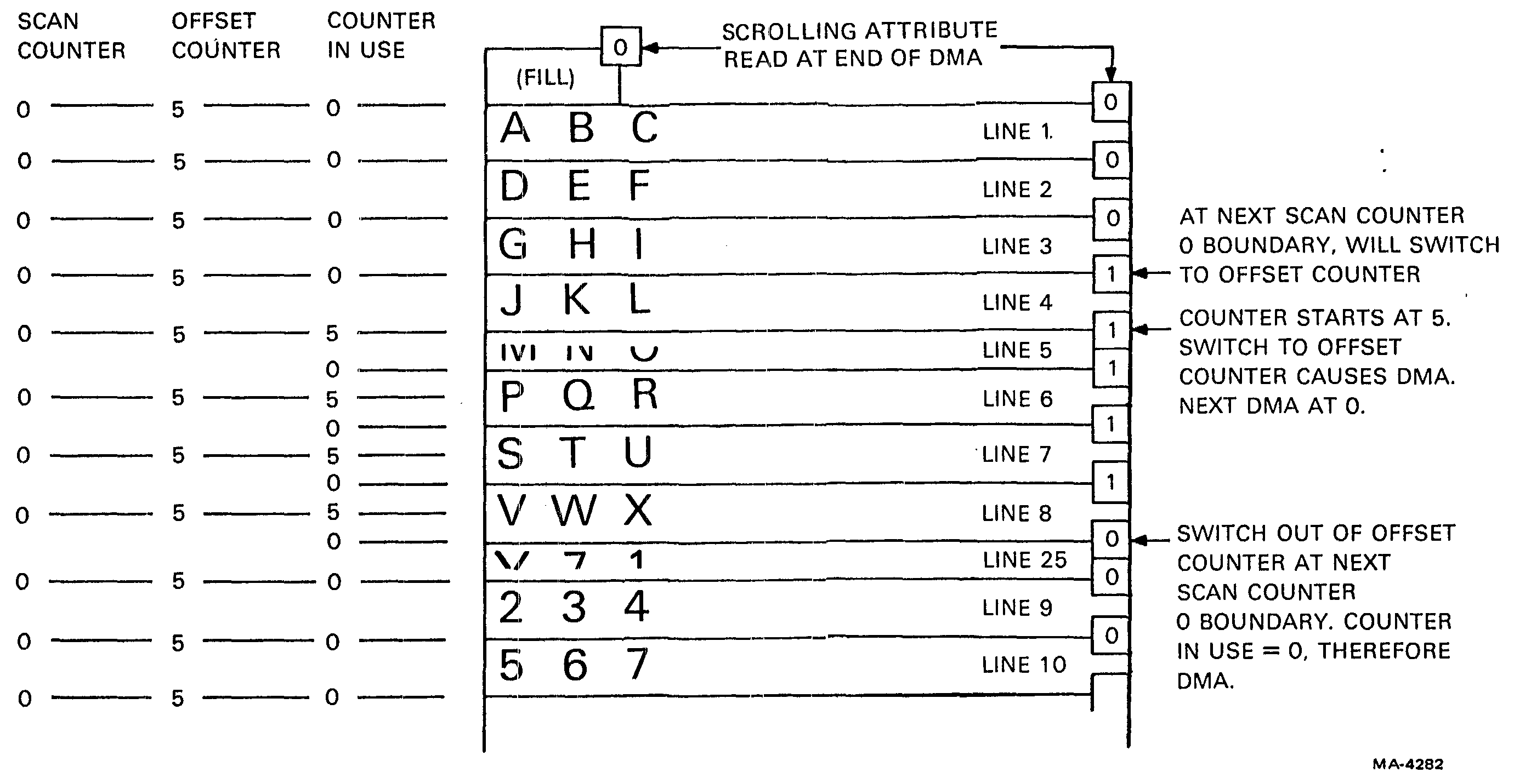
The scrolling attribute bit on line 4 enters the DC012 during the DMA. However, it does not cause the MUX to switch until scan 0 of the next line. Because of the switch to the offset counter, line 5 begins with a DMA but it starts displaying with scan 5 because of the offset counter. Its attribute bit enters the DC012 at the end of the DMA. Five scans later the counter in use is 0, so another DMA occurs. Because the scan counter did not reach 0 before the DMA, the scrolling attribute bit from line 5 is ignored. Line 6 DMAs and its attribute bit enters the DC012. Line 6 is present for all 10 scans and so as the scan counter passes through zero, the DC012 accepts control from the line 6 attribute bit. This special case (pointer to the second line in the scrolling region while the smooth scroll is in progress) is the only occasion when an attribute bit is ignored. The double height and width bits in the same byte are accepted at the moment the DMA for the corresponding line begins.
As line 5 begins to roll off the screen, the extra line in memory, line 25, becomes visible. It becomes the new line 8 when line 5 is gone. Line 25 carries a non-scroll attribute bit because the next line (which the address on line 25 points to) is not in the scrolling region. Line 25 was DMA’d in when the counter in use was 0 so it starts with its top scan. But the attribute bit is accepted when the scan counter reaches 0 five scans later. Now the counter in use is 0 again because of the shift back to the scan counter so another DMA occurs, bringing in line 9, which also carries a non-scroll attribute bit. The rest of the screen thus appears in non-scroll fashion.
The microprocessor keeps a running account of the cursor position. It starts at the reset position, line 1 - column 1 (top left corner) and responds to any change in position that might result from receiving a new character, a cursor position command, a line feed, etc. The microprocessor calculates the appropriate screen RAM address from the combination of previous line and column plus change in position, or from the specified line and column in a direct cursor address (DCA) control sequence. The microprocessor then records the current setting of the base attribute bit of the character at that address and then periodically inverts the attribute bit, showing the operator that the cursor is located at the spot on the screen where the attribute appears and disappears.
When a line scrolls on the screen, its location in RAM remains the same. To keep the cursor at the same screen location as before, representing the cursor moving down through the lines, the microprocessor calculates a new address for the cursor at the same column number but in the RAM location corresponding to the next line. Then, after resetting the attribute at the old location to its original value, it records and then toggles the attribute bit at the new location.
The attribute bit that the microprocessor toggles and the appearance on the screen depend on the setup selection of the cursor attribute and on the absence or presence of the AVO. If the AVO is not installed, the microprocessor toggles the eighth bit in each character word. A setup selection of reverse video causes the microprocessor to set the DC012 to interpret its base attribute input (REV VID H) as reverse video. If setup specifies that underline is to be used for the cursor, the DC012 is set to interpret the base attribute as underline instead of reverse. Notice that without the AVO the cursor selection determines the appearance for all characters on the screen that have the attribute asserted. Furthermore, the microprocessor will accept the commands for either reverse or underline to assert the attribute.
With the AVO present, the microprocessor tells the DC012 to interpret the base attribute as reverse video. The cursor selection in setup determines whether the microprocessor toggles the base attribute bit (eighth character bit) to get reverse video or one of the bits in the AVO RAM to get underline. With the AVO present, cursor selection is independent of attributes and all attributes are available at the same time.
The SET-UP area is a portion of the scratch RAM. It contains 8-bit bytes that are passed between the RAM and the NVR. Here is a list of the SET-UP area contents. This list is subject to change.
| 22 bytes | Answerback message (20 characters and 2 delimiters) |
| 17 bytes | Tabs encoded in bits |
| 1 byte | 80/132 column mode |
| 1 byte | Intensity |
| 1 byte | Mode byte for PUSART |
| 1 byte | On-Line/Local |
| 1 byte | Switchpack 1 (scroll, autorepeat, screen, cursor) |
| 1 byte | Switchpack 2 (bell, keyclick, ANSI/VT52, XON /XOFF) |
| 1 byte | Switchpack 3 (US/UK #, wrap, new line, interlace) |
| 1 byte | Switchpack 4 (parity sense, parity, bits/char, power) |
| 1 byte | Switchpack 5 (STP - visible only when option installed) |
| 1 byte | Transmit baud rate |
| 1 byte | Receive baud rate |
| 1 byte | Parity |
| 1 byte | Checksum for NVR |
When the SET-UP key is pressed, the SILO locks and any scroll in progress is allowed to finish. Now the 25th line (Extra) is available for one of the lines at the bottom of the screen. Another 135 bytes are available as line Extra2 for use as the other of the two bottom lines, or for the NVR buffer area and the “Wait” message displayed during NVR operations. Another 125 bytes are the SET-UP screen RAM. They store the words “SET-UP A” twice (for double height) and the words “To exit press SET-UP” with the three lines’ terminator and address bytes, plus 19 more terminators and addresses for the 19 blank lines in the middle of the SET-UP screen.
For SET-UP A, the microprocessor performs a routine to fill the line at the bottom of the screen with a ruler. The other free line displays the cursor and letters “T” to indicate tab positions. Then the microprocessor counts from the beginning of the tab bytes in the SET-UP area to find the bit corresponding to the column number where the cursor is. If the bit is set, the microprocessor writes the letter “T” in the current cursor position. Keys (Set/Clear Tab, Clear All Tabs) on the keyboard can toggle the setting of the bit in the SET-UP area, and the microprocessor writes or erases the “T” to agree.
For SET-UP B, the microprocessor displays the data contained in the switchpack and baud rate area by writing corresponding information into the bottom line. Switch pack 5 is only displayed if the Option Present flag is asserted at the STP. The other free line is not written into but is used to display the cursor position and to display the answerback message when the message is being entered. The switchpack data is changed by a key on the keyboard (Toggle 1/0).
The non-switchpack data is changed by separate keys. These include parameters that display themselves - line/local (displayed in the LEDs) and 80/132 column, seen on the screen. Transmit and receive are displayed numerically as is parity in later models. Switching between SET-UP fields and starting Reset can also be done with separate keys on the keyboard.
Two monitors have been used in VT100 production. Early VT100s used DEC part number 30-14590. Later terminals used DEC part number 30-16080. Most of the circuitry in these monitors is standard television technique, and this description simply highlights the signal path. An overview of the general principles of the horizontal section is included because this circuit is not intuitively understandable from an examination of the schematic. It is also the likely candidate for failure because of high stresses in the components.
The cathode driver stage gets its operating supply of 38 volts from a winding of the flyback transformer. R108 is the collector load resistor. C101 bypasses the emitter resistor to improve high frequency response. The stage is intended to be biased by the driving circuit (direct video out in the terminal controller). R105 couples the video signal to the cathode limiting current flow if the CRT arcs.
The brightness control circuit gets its -150 volt operating supply from the horizontal output circuit. A charge pump (C104, C105, CR103, CR104) produces a large negative voltage by inverting the large positive swings in the stage. The brightness voltage returns to the +38 volt video output power supply, rather than ground, to allow the brightness control output to vary from -42 to +17 volts. The brightness control potentiometer R109 varies the bias on the first grid of the CRT. C107 bypasses currents resulting from internal CRT arcs from the high voltage anode and also bypasses video signals from the grid to ground.
The vertical oscillator receives its synchronizing drive through inverter-buffer Q298. R331 and C314 are a low pass filter on the input for noise immunity. The input is ac-coupled so that if the drive stops in either a high or low state, the circuit can self-oscillate to keep the beam moving on the CRT.
Basically, the oscillator is an RC timer with R333 and R334 through CR304 charging a capacitor made of C318 and C319 in series. As the voltage across the capacitor rises, emitter follower Q309 drives the output amplifier Q310 so that its collector current rises at the same rate. CR304 is two diode drops to compensate for the drops in Darlington Q309 so the voltage at the base of Q310 is the same as the voltage at the top of C318. When Q308 receives a vertical drive pulse, it discharges the capacitor.
R341 and R342 are positive feedback to the junction of C318 and C319. As Q310’s emitter voltage rises with increasing current, the two resistors couple that voltage back to the timing capacitor. This makes the voltage across the capacitor rise faster than it would with only the charging current from R333 and R334. But because the rise in capacitor voltage causes Q310 to turn on more, the feedback voltage increases as well. The exponential rise in Q310’s output current that results closely matches the variations in L301’s current. This is explained more under Linearization (Paragraph 4.8.1.6).
If the vertical circuit does not receive a drive signal, it oscillates by itself to keep the electron beam moving to prevent a phosphor burn. The self-oscillation period is longer than the period between vertical drive pulses so the drive pulses, when present, always control the vertical scanning rate.
Without a drive signal, Q308 is off. The regular RC circuit produces a rising voltage at the base of Q310. While Q310’s output moves the electron beam, its base voltage is coupled to Q308 through R335 and CR302. When the voltage rises above the diode drops of CR302 and Q308 base-emitter junction, Q308 turns on, discharging the timer and cutting off Q310. The retrace voltage that forms at L301 is coupled by R344, C316, and R339 back to Q308 to keep it on long enough to complete a retrace even though the voltage from Q310’s base (that started the cycle) has started to decrease. After the voltage at L301 falls (due to current flow to the yoke), the drive to Q308 is gone, Q308 turns off, and the self-oscillation cycle begins again.
Consider L301, which is a large inductor, to be a constant current source. Assume that the yoke starts with a current that deflects the beam to the top of the screen, and Q310 is off. The current flows out of L301 through C321 and into the yoke. Q310 now turns on with a gradually rising voltage on its base. Q310 thus draws an increasing amount of current from the junction of L301 and the yoke. Because L310’s current is relatively constant, this means that less current is available for the yoke, so as Q310’s current increases, the yoke’s current decreases. Eventually Q310 passes all of L301’s current and the yoke current is 0 with the beam in the center of the screen. As the current in the collector of Q310 increases further, the current in the yoke reverses and adds to the current coming from L301. This opposite current deflects the beam toward the bottom of the screen. Now the vertical drive pulse turns Q310 off, and L301 produces a large positive voltage to try to maintain its constant current. This voltage rapidly reverses the current in the yoke and makes the beam return to the top of the screen very fast. Q310 turns back on and the cycle repeats.
C320, R338, and R340 limit the voltage across L301 during vertical retrace.
Because L301 is not an infinitely large inductor, it is not a perfect current source. Current through it decreases gradually until the beam reaches the center of the screen and then increases again toward the end of the cycle. This non-ramp component of the current would cause character height to vary from top to bottom if allowed to pass to the yoke. The exponential drive to Q310 as a result of feedback causes Q310 to accept the varying current from L301 at the same time that a ramp current through the yoke is maintained.
The horizontal driver receives a TTL level drive pulse from the terminal controller. R468 limits the base current to Q413. C435 provides noise immunity for the drive input.
When the input is high, Q413 is on. With pin 6 of transformer T403 pulled low by Q413, and with about half the supply voltage at pin 4, there is approximately 6 volts across the primary winding 4-6. The secondary winding 3-2 sees one quarter of this voltage across itself due to the 4:1 turns ratio, but no current flows because Q414’s base-emitter junction is reverse biased. Meanwhile, current increases through winding 4-6 while Q413 is on, storing energy in T403's core. When the drive signal falls, turning Q413 off, winding 3-2 reverses polarity. Current now flows from T403 winding 3-2 through Q414’s base-emitter junction, Q414 saturates, and the horizontal output functions as discussed below.
When the drive signal goes high again at the beginning of horizontal retrace, Q414 needs to turn off very quickly to minimize dissipation. The purpose of opposite polarities in T403 is to force Q414 off by turning Q413 on. When Q413 turns on, winding 3-2 reverses polarity again and this voltage forces Q414’s base-emitter junction into a reverse biased state, rapidly discharging Q414’s stored base charge and cutting off Q414’s collector current.
R470 limits the peak current through Q413. R470, and R471 (if present), limit the on time of Q414. C443 (if present) speeds up the turn-off of Q414. C436 limits the peak voltage that develops across Q413 caused by leakage inductance in the primary of T403 that prevents complete coupling of the primary energy into the secondary. C437 filters Q413’s power supply.
The horizontal output circuit consists basically of Q414, CR406, C438, C441, and the horizontal deflection yoke. Assume that the beam is at the center of the screen during a scan. Refer to the waveform diagram (Figure 4-8-5) for reference points T0 through T4.
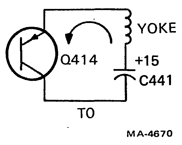
| T0: | Right Half of Scan (Figure 4-8-1) |
|---|---|
| Initial Condition: | Current through the yoke is zero. C441 is charged to +15 volts. Q414 is on. |
| Action: | Current now flows out of the yoke through Q414, pushed by the voltage across C441. The voltage across C441 is nearly constant so the current through the yoke’s inductance increases linearly. As the current increases, the beam moves to the right of the screen. The magnetic field building in the yoke stores energy. |
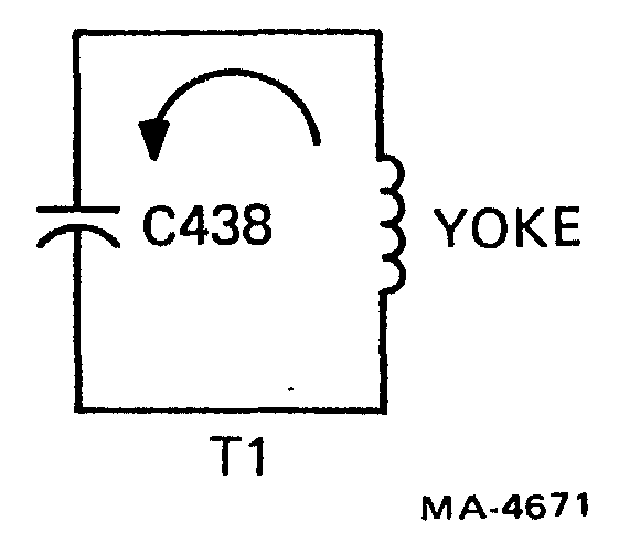
| T1: | Start of Retrace (Figure 4-8-2) |
|---|---|
| Initial Condition: | Current out of the yoke is maximum. Q414 is switched off. C438, which had been grounded by Q414, has 0 volts across it. |
| Action: | Current continues to flow out of the yoke by inductive inertia as the stored magnetic field collapses. C438, which is a small valued capacitor, quickly charges to a high voltage. This voltage opposes current flow and causes a rapid reduction in current. The beam quickly returns to the center of the screen. |

| T2: | Middle of Retract (Figure 4-8-3) |
|---|---|
| Initial Condition: | Current through yoke is zero. C438 is charged to +175 volts. |
| Action: | The high voltage across C438 causes a rapid rise in current into the yoke. The beam moves to the left of the screen. |
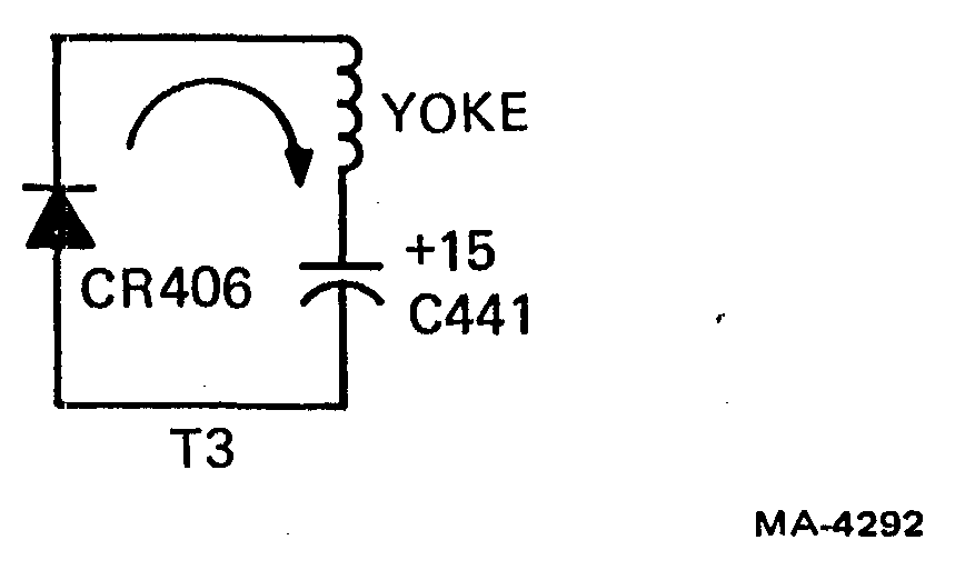
| T3: | Start of Scan (Left Half) (Figure 4-8-4) |
|---|---|
| Initial Condition: | Current into the yoke is maximum. C438 is discharged. |
| Action: | Inductive inertia makes the top of the yoke slightly negative, forward biasing CR406 to provide a return path for current out of the bottom of C441. The yoke current gradually decreases as the magnetic field collapses and discharges into C441 against the voltage across C441. The beam moves to the center of the screen. |
| T4: | Return to T0 |
|---|
(Refer to Figure 4-8-5.) L403 adds a variable inductive reactance that controls current in the circuit to vary the scan width. L402 is a magnetically biased inductor whose reactance varies nonlinearly with changes in yoke current. This, with R481 and C442, provides correction for nonlinearity caused by the decaying exponential rate of current increase in the yoke caused by the yoke’s resistance. It does this by allowing more voltage across the yoke at the end of the scan. This is needed because as current increases, the voltage drop increases across the resistance of the yoke, tending to reduce the rate of current increase.
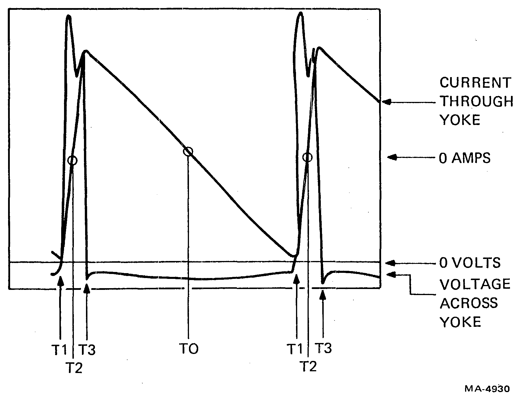
Power enters the circuit through the primary of the flyback transformer. CR408 and C439 work with an autotransformer winding on the primary to boost the stage’s operating voltage to +15 volts. The output circuit shuttles yoke current back and forth between C438 and C441, losing only a small amount of power in resistive losses. Therefore, the average current through the flyback primary is small (approximately 800 mA). C438 is relatively small so that the voltage drop across its reactance can provide “S” correction for the horizontal scan. This compensates for the difference between the arc of the tube face and the arc of the beam’s deflection. Each time Q414 turns off, a 175 volt pulse, lasting the interval of horizontal retrace, appears at the dotted end of the flyback primary. This pulse passes into the flyback secondary to provide high voltages for the CRT.
When the 175 volt pulse appears on the flyback primary at retrace, the flyback secondary produces 12 kV which is rectified by CR407 and filtered by the capacitor made by the aquadag (graphite) coatings on the inside and outside of the CRT’s glass envelope. Screen and focus grid voltages of about 370 volts come from a lower voltage winding on the flyback and are rectified by CR409. For the cathode driver, 38 volts comes from another winding and is rectified by CR102.
The video amplifier consists of Q101 and its associated circuitry. The incoming video signal is applied to the monitor through J101-8 and R101 to the base of Q101.
Transistor Q101 has a nominal gain of 15, and operates as a class B amplifier. Q101 remains cut off until a dc-coupled, positive-going signal arrives at its base and turns it on. R103 provides series feedback that makes the terminal to terminal voltage gain relatively independent of transistor parameters and temperature variations. R102 and C101 provide emitter peaking to extend the bandwidth to 12 MHz.
The negative-going signal at the collector of Q101 is direct coupled to the CRT cathode. The class B biasing of Q101 allows a large video output signal to modulate the CRT’s cathode and results in a maximum available contrast ratio.
Overall brightness of the CRT screen is also determined by the negative potential at its grid which is varied by the brightness control.
Q102 is a thyristor used as a programmable unijunction transistor and with its external circuitry forms a relaxation oscillator operating at a vertical rate. The sawtooth forming network consists of A101, C103, and C104. These capacitors charge exponentially until the voltage at the anode of Q102 exceeds its gate voltage at which time Q102 becomes essentially a closed switch, allowing a rapid discharge through L101. The rate of charge or frequency is adjustable by A101. The oscillator is synchronized by a negative pulse coupled to its gate from the vertical drive pulse applied externally at J101-9.
A divider network internal to A101 sets the free running frequency by establishing a reference voltage at the gate. This programs the firing of Q102 and amounts to resistive selection of the intrinsic standoff ratio. Frequency is controlled by passive components only. CR101 provides temperature compensation for Q102 while controlling the gate impedance to allow easy turn on and off of Q102. L101 forms a tuned circuit with C103 and C104 during conduction of Q102 which provides a stable control on the dropout time of Q102 to assist in maintaining interlace. Q103 collector to base forward diode clamping action prevents the voltage from swinging too far negative during this flywheel action.
The sawtooth at the anode of Q102 is direct coupled to the base of Q103. This stage functions as a Darlington pair emitter follower driver for the output stage Q104. It presents an extremely high impedance in shunt with A101 and prevents the Beta dependent input impedance of Q104 from affecting the frequency of the sawtooth forming network.
Linearity control of the sawtooth is accomplished by coupling the output at Q103 emitter resistively back into the junction of C103 and C104. This provides integration of the sawtooth and inserts a parabolic component. The slope change of the sawtooth at Q103 output is controlled by the setting of A102. The output at Q103 is coupled into a resistive divider.
Height control R110 varies the amplitude of the sawtooth voltage applied to the base of Q104 and controls the vertical raster size on the CRT. C105 limits the amplitude of the flyback pulse at Q104 collector.
The vertical output stage Q104 uses an NPN power transistor operating as a class AB amplifier. The output is capacitively coupled to the yoke. L1 provides a dc connection to B+ for Q104. It has a high impedance compared to the yoke inductance that causes most of the sawtooth current of Q104 to appear in the yoke. R114 prevents oscillations by providing damping across the vertical yoke coils.
The purpose of Q105 and Q106 is basically to process the incoming horizontal drive signal into a form suitable to drive the output stage Q108. The duty cycle of Q108 becomes essentially independent of the amplitude and pulse width of the drive pulse. This is a necessary condition to assure stability and reliability in the output stage. In addition, these stages provide a horizontal video centering adjustment by delaying retrace with respect to the horizontal drive pulse.
The drive pulse is presented to Q105 via J101-6. The base circuit of Q105 includes a clamp and a differentiator that makes Q105 output insensitive to drive pulse amplitude and width changes. The only requirement is that pulse amplitude be of 2.5 volts minimum and pulse width should be 10 to 40 microseconds. Q105 with Q106 functions as a monostable multivibrator with Q107 being a slave that provides a positive feedback. Specifically, when Q105 is turned on by the drive pulse, it discharges C112 at a rate determined by the setting of A103. When C112 is discharged to 1.75 volts, Q106 turns off. This change of state turns Q107 on and the base drive to Q106 from R128 is shunted through Q107. Q106/Q107 remains in this state for nominally 2S microseconds until C112 recharges through A103 to 8.25 volts. At this time, Q106 is biased on again by the current through A103. The multivibrator is now in a state in which Q106 is on and Q105/Q107 is off. It remains in this state until the next drive pulse occurs or power is turned off. C112 is the only timing capacitor in the circuit and has two time constants associated with it. Primarily, the charge path between pin 1 and pin 3 of A103 determines the on time of Q107. The discharge path through the video centering control and Q105 determines the delay between application of the drive pulse and the start of retrace (turn on of Q107).
These stages consist of Q107 driving the output stage, Q108, and its associated circuitry through T101. Q107 is an inverting slave of Q106 and is driven alternately into saturation and cutoff as are all stages in the horizontal circuit. Q107 output is transformer coupled to the output stage with phasing of T101 chosen such that Q108 turns off when Q107 turns on. This allows Q108 to turn off quickly, thus minimizing dissipation. A careful review shows that Q108 turns off at a variable delay time after receipt of the drive pulse. This action causes retrace to begin.
During conduction of the driver transistor, energy is stored in the coupling transformer. The polarity at the secondary is then phased to keep Q108 cut off. As soon as the primary current of T101 is interrupted due to the base signal driving Q107 into cutoff, the secondary voltage changes polarity. Q108 now saturates due to the forward base current flow. This gradually decreases at a rate determined by the transformer inductance and circuit resistance. However, the base current is sufficient to keep Q108 in saturation until the next polarity change of T101.
The horizontal output stage has two main functions:
Q108 acts as a switch that is turned on or off by the rectangular waveform on the base. When it is turned on, the supply voltage plus the charge on C123 causes deflection current to increase in a linear manner and moves the beam from near the center of the screen to the right side. At this time, the transistor is turned off by a polarity change of T101 that causes the output circuit to oscillate. A high reactive voltage in the form of a half cycle negative voltage pulse is developed by the deflection coil inductance and the primary of T2. The peak magnetic energy that was stored in the deflection coil during scan time is now transferred to C122 and the deflection coil distributed capacity. During this cycle, the beam is returned to the center of the screen.
The charged capacitances now discharge into the deflection coil and induce a current in a direction opposite to the current of the previous part of the cycle. The magnetic field thus created around the coil moves the scanning beam to the left of the screen.
After slightly less than half a cycle, the decreasing voltage across C122 biases the damper diode CR111 into conduction and prevents the flyback pulse from further oscillation. Magnetic energy that was stored in the deflection coil from the discharge of the distributed capacity is now released to provide sweep for the left half of scan and to charge C123 through the rectifying action of the damper diode. The beam is now at the center of the screen. The cycle repeats as soon as the base of Q108 becomes positive with respect to its emitter.
C123 serves to block dc current from the deflection coil and to provide “S” shaping of the current waveform. “S” shaping compensates for stretching at the left and right sides of the picture tube because the curvature of the CRT face and the deflected beam do not follow the same arc.
L103 is an adjustable width control placed in series with the horizontal deflection coils. The variable inductance allows a greater or lesser amount of deflection current to flow through the horizontal yoke and varies the width of the horizontal scan.
Linearity control is provided by modifying the deflection coil voltage. During retrace, an auxiliary winding on the flyback transformer supplies a pulse that charges C119 through rectifier diode CR112 and L102. This voltage is then applied in series with the deflection coil when the damper diode turns on at the start of trace. The voltage is sawtooth shaped and has the effect of decreasing the deflection coil current as a function of the sawtooth shape. This compensates for the stretch normally found on the left side of the screen due to the deflection coil and system RL time constant. Linearity is optimized by adjustment of L102 that acts as an impedance to the pulse from T2.
The negative flyback pulse developed during horizontal retrace time is rectified by CR110 and filtered by C117. This produces approximately -130 Vdc which is coupled through the brightness control R117 to G1 of the CRT.
This same pulse is transformer-coupled to the secondary of T2 where it is rectified by CR2, CR113, and CR114 to produce rectified voltages of approximately 12 kV, 400 V, and 32 V respectively. 12 kV is the anode voltage for the CRT, 32 V is used for the video output stage, and the 400 V source is used for G2 and G4 voltages for the CRT.
The VT100 series power supply is a switching supply that has 95 watts capacity with four separate voltage outputs. Figure 4-9-1 is a block diagram of the power supply.
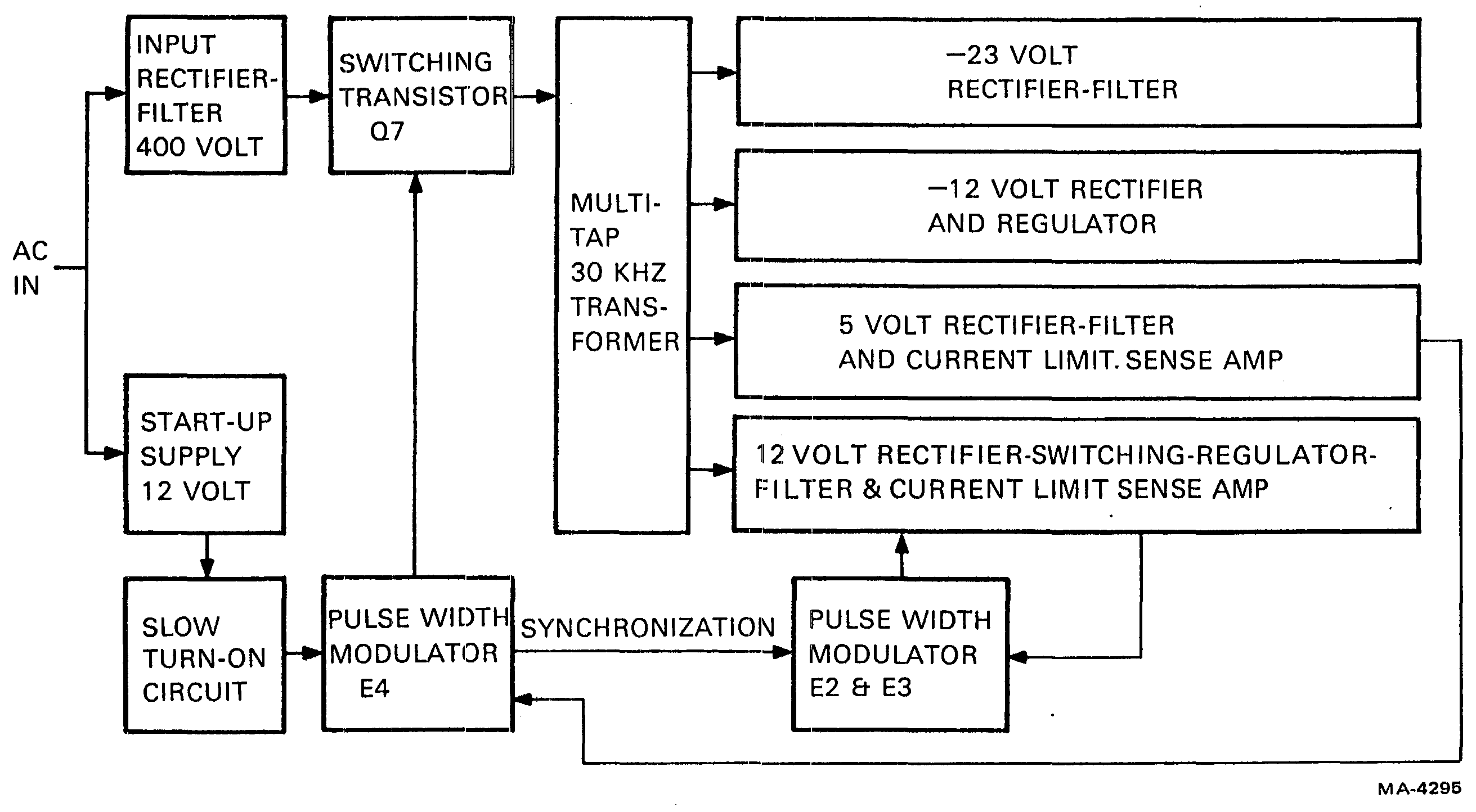
The input to the supply consists of an electromagnetic interference (EMI) filter, an on/off switch, a fuse, and a 120/230 volt select switch. Either on 120 Vac or 230 Vac input, thermistors R1 and R50 reduce the start-up inrush currents to safe levels. For 120 Vac operation a voltage doubler rectifier is used; for 230 Vac operation a full wave bridge rectifier is used. The storage voltage across both C9 and C14 varies with the input line voltage from 200 to 360 Vdc. R19 and R20 are bleeder resistors.
Transformer T2 is a start-up transformer that supplies the power to start the control circuit. The ac voltage on the primary of T2 is stepped down, rectified, and filtered by C33. The dc voltage is applied to the input of +12 volt regulator Z2. The output passes through two diodes D24 and D25 to the control circuitry. When the unit is turned on, the only voltage supplying power to the control circuit is from the regulator Z2. After the outputs come up, the +12 output is fed back through diode D34 to the control circuitry. This voltage, being higher than that delivered by the start-up circuit, will back bias D24 and D25, isolating the Z2 regulator. This scheme of returning the output through D34 enables the power supply to also meet its ride-through specification (ability to supply power during brief outages).
The control circuit in the VT100 power supply is designed around the 3524 pulse width modulator (PWM) IC. It houses a voltage reference, error amplifier, oscillator, pulse width modulator, pulse steering flip-flop, dual alternating output switcher, current limit circuit, and a shutdown circuit. Refer to the regulator IC block diagram in Figure 4-9-2 and the power supply timing diagram in Figure 4-9-3.
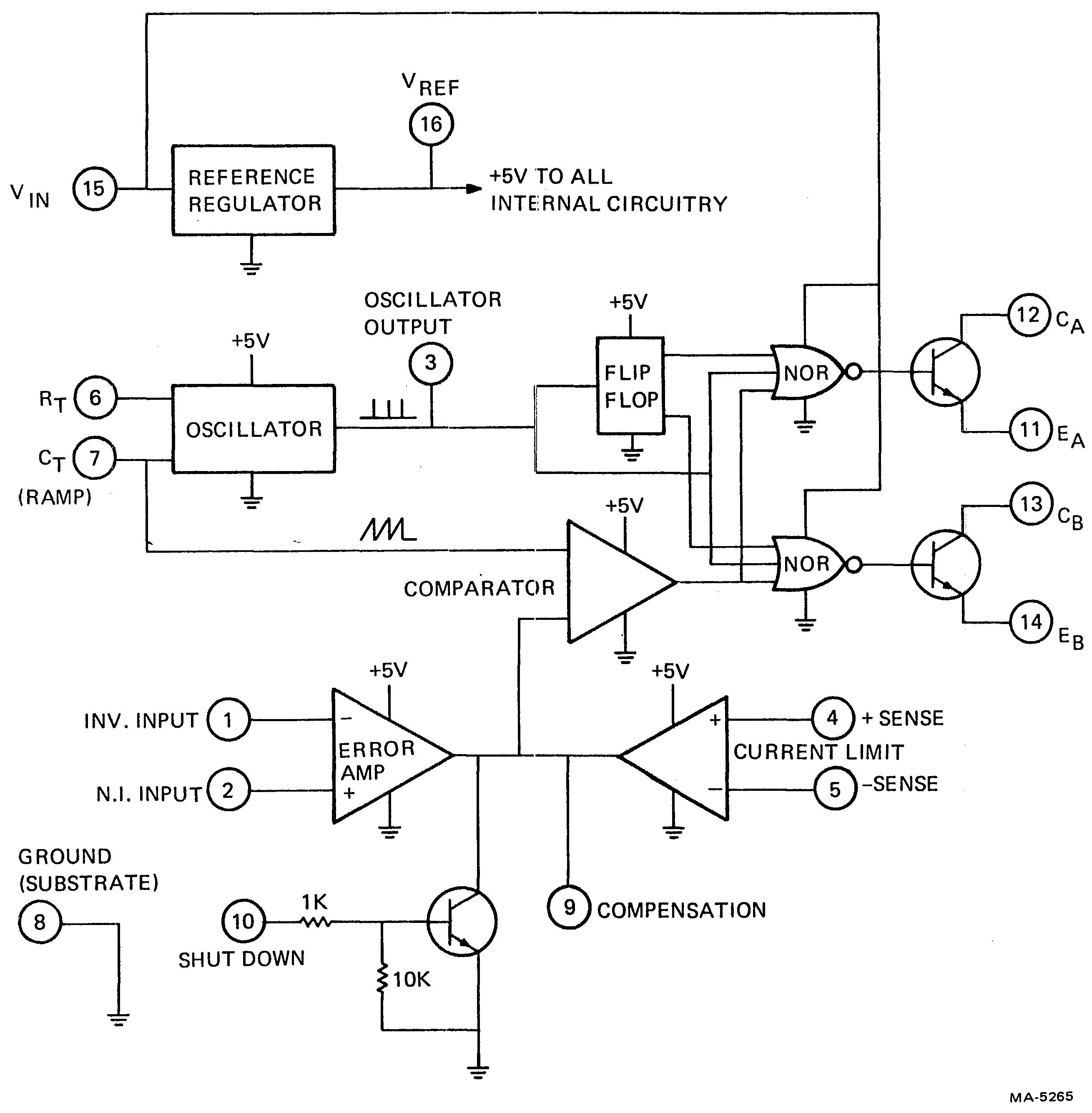
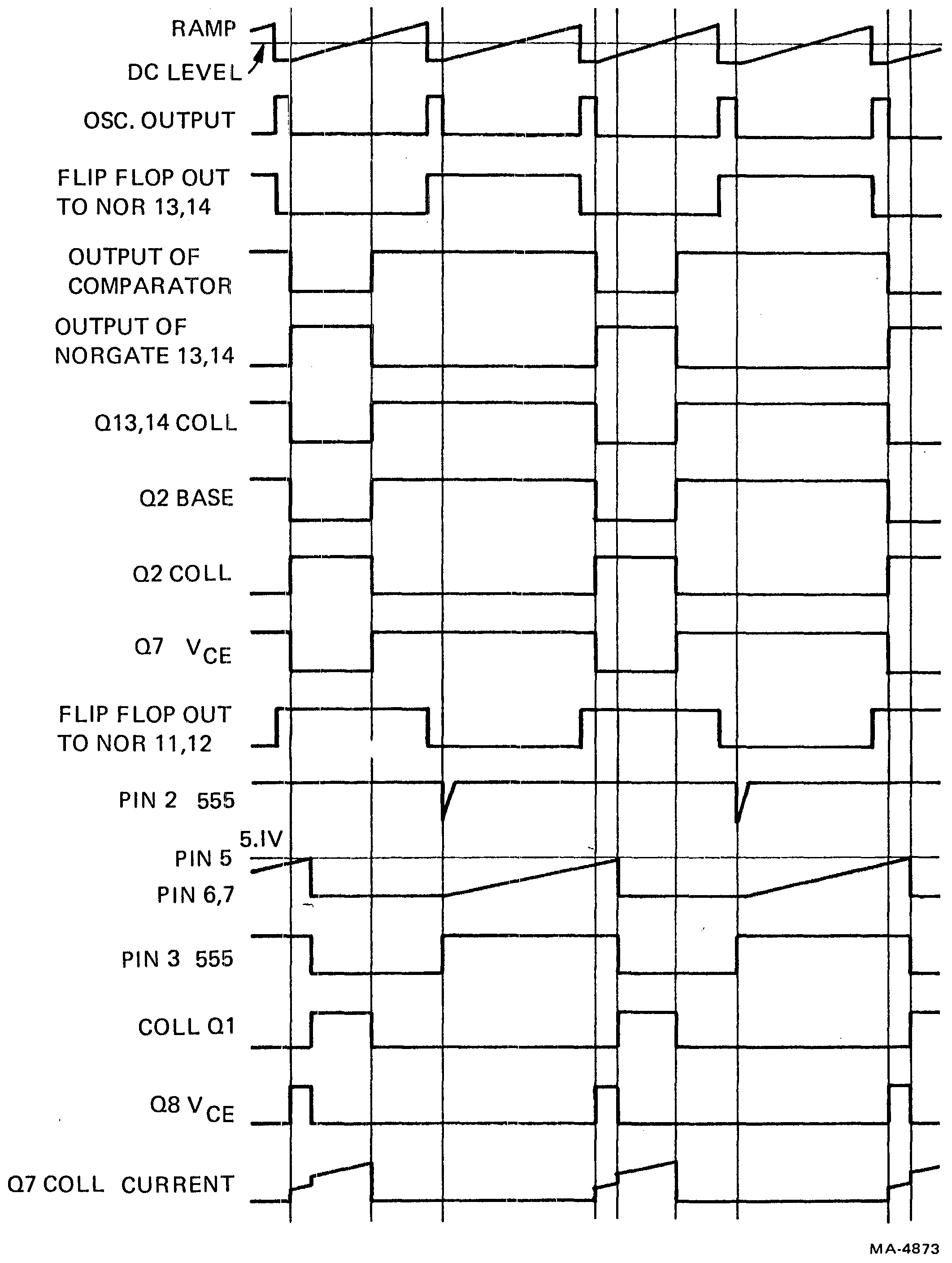
The oscillator frequency is determined by resistor R18 and C7. The ramp generated by C7 is used as a reference for the comparator. The discharge time of C7 determines the pulse width of the oscillator output pulse. This pulse is used as a blanking pulse to ensure that the outputs of the 3524 cannot turn on simultaneously. Capacitor C5 ensures that the blanking pulse is wide enough.
The error amplifier in the 3524 is a transconductance amplifier with an output (pin 9) impedance of approximately 5 megohms. Pin 9 is a convenient point to place the compensation network, R30, C17 and R13. It is also an ideal point at which to turn off the switching regulator and also to put the slow-turn-on circuit. The slow-turn-on circuit consists of D39, R51, D40, and C34. When the power supply is initially turned on, pin 9 is pulled to ground by C34 through D39. As C34 charges slowly and exponentially, pin 9 follows, turning the power supply on slowly and exponentially. The current that charges C34 comes from pin 9 and the +12 volt start-up. Pin 9 operates at a dc level that is determined by the input error voltage into the amplifier. C34 eventually charges to +12 volts, thus back biasing D39. When the supply is turned off, C34 discharges through D40, allowing the supply to be ready for another soft start.
The inverting side (pin 1) of the input to the error amplifier is tied to the +5 volt output through a dividing network, R32 and R48. The noninverting side (pin 2) is referenced to a 5.1 volt zener, D38, through a divider network, R41 and R49. An error appearing at the input causes pin 9 (output of the error amplifier) to shift. This dc level shift is tied into an input of a comparator. As mentioned earlier, the ramp generated by C7 is tied into the other input of the comparator. This is the means by which the regulator is pulse width modulated. The actual frequency of the oscillator is 60 kHz. The switching frequency of the power supply is one-half that of the oscillator, 30 kHz, because only one of the single-ended outputs is used. This output, pin 13, a pulse width modulated wave, turns transistor Q4 on and off. When Q4 is off, Q3 supplies base current to Q2, turning it on. D7 and D8 are antisaturating diodes. R14 limits the base drive, and R15 and C4 are a speed-up circuit to turn Q2 on and off fast. When Q2 is on, Q7 (high voltage switch) is off. Current flows from +12 through R11, D6, and winding 5,6 of pulse transformer T3 through transistor Q2 to ground. The circuit remains in this state until the base drive to Q2 is removed by the control circuit. When Q2 turns off, the voltage across T3 winding 5,6 reverses, causing all the dotted ends of windings in T3 to become negative. Current starts to flow into the base of Q7. This causes collector current to flow. This current flows through winding 1,2 of T1, through the transistor and winding 2,1 of T3. The current in winding 2,1 of T3 produces current flow in windings 3,4 and 7,8 of T3. The action that takes place is regenerative and causes Q7 to snap on. When Q7 conducts, energy is transferred from the primary of T1 to the secondary. The positive voltage at terminal 5 of T1 charges capacitor C6 through D14 and R21. The voltage at terminal 5 depends on the conduction time of the switch. When the control circuit switches Q2 on, C6 discharges through D9, winding 5,6 of T3 and transistor Q2. The current through winding 5,6 of T3 makes all dotted ends positive on T3. The negative polarity on the base of Q7 turns it off. D11 is across T3 and Q2 for noise immunity. Diodes D41, D12, and D3 are antisaturation diodes. C19, R27, and D27 form the snubbing network.
Winding 1,3 of T1 is a reset winding. On turn-off, this winding clamps the collector of Q7 to two times the storage voltage. It is also used for resetting the high frequency transformer core.
There are four secondary outputs. The -23 volt output is rectified by D28, filtered by C18, and passed on through a 300 ohm resistor. The output goes to two zeners mounted on the video board. The 300 ohm resistor limits power dissipation in the zeners and also dissipates all power under short circuit conditions.
The -12 volt output consists of a rectifier diode (D29), filter capacitor (C20), and a regulator Z1.
The voltage at winding 9,10 of T1 is rectified by D36 and goes into an averaging network L2 and C31.
The catch diode, part of D36, completes the conduction path when Q7 is off. When Q7 is on, there is a voltage on the secondary with pin 9 being positive. D36 is forward biased and current flows through L2. This causes the inductor current to increase at this time. With the switch open, stored energy in the inductor forces the current to continue to flow to the load and return through the catch diode (D39). The voltage across L2 is now reversed and is approximately equal to the output voltage. During this time the current in L2 decreases. The average current through L2 equals the load current. Since C31 keeps the output voltage constant, the load current will also be constant.
The +12 volt output circuitry works the same way as above except the voltage at winding 4,5 is turned on by Q8 and turned off by the voltage at terminal 5 going negative.
The current limit circuits for the +5 and +12 outputs have identical configurations; only some resistance values differ. The voltage at pin 5 of the comparator referenced to the junction of R16 and R37 is compared to the voltage drop across R37. When the voltage across R37 increases to a point where pin 6 is more positive than pin 5, E1 switches and pin 7 goes low, pulling pin 9 of E4 to ground and thus turning off the switching regulator.
The +12 volt control circuitry is synchronized to the 3524 pulse width modulator at a 30 kHz rate. When pin 12 of E4 is high, capacitor C15 charges up from the +12 start-up through R29, R26, and D13. The polarity on the capacitor is such that when pin 12 of E4 goes low, the emitter of Q6 is pulled negative with respect to the base which is at ground. Q6 saturates, pulling pin 2 of E3 down, thereby allowing the ramp generated at pins 6 and 7 by C13 to ramp up. Pin 6 is the threshold pin. The input to this pin is compared to the voltage at pin 5. When the voltage at pin 6 is equal to that of pin 5, pin 7 discharges capacitor C13 and pin 3 of E3 goes low. Whenever the voltage at pins 6 and 7 is ramping up, the output of E3, pin 3, is high.
C13 is the timing capacitor for the +12 volt pulse width modulator. C13 is charged from a voltage-controlled current source. The voltage at pin 5 of E3 is connected to the 5 volt reference. Thus, when the voltage across C13 reaches 5 volts (pin 6 of E3), the output of E3 pin 3 drops low, turning Q1 off and thereby turning Q8 on. Q7 and Q8 are turned off simultaneously when Q2 is turned on. The pulse width that determines the length of time Q8 is on is determined by the rate of voltage rise on capacitor C13. The faster C13 charges, the longer Q8 conducts. The error voltage that determines the rate of rise on C13 is generated by error amplifier E2. The noninverting input of the error amplifier is referenced to D38, a 5.1 volt zener. The inverting input is divided up by R2 and R3 and senses the +12 volt output. Any difference creates an error signal on pin 6 of E2. This increase or decrease in voltage at pin 6 divided by R33 generates a proportional change in current through Q5, thereby changing the rate of voltage charge on capacitor C13. As described above, the change in rate of charge affects the pulse width.
R4, C1, and R5 are the compensating components of error amplifier E2. D1 and D2 are antisaturating diodes. R6 limits the base drive and R7 and C3 are a speed-up circuit to turn Q1 on and off.
| Voltage | |
|---|---|
| Single phase, 2 wire | 90-128 V rms (switch-selected) 180-256 V rms |
| Frequency | 47-63 Hz |
| Current | 2.2 A rms max. @ 115 V rms; 1.1 Arms max. @ 230 V rms. |
| Input power | 250 VA apparent 150 W max. |
| Power factor | Ratio of input power to apparent power is greater than 0.6 at full load and minimum input voltage. The VT100 appears capacitive to the line. |
| Leakage current | When installed in VT100 terminal, current to ground is 0.5 mA max. Each line to ground at 250 V rms sine, 50 Hz. |
| Current limiting | When installed in video terminal, 3.0 A normal blow fuse. |
| Electrical Magnetic Interference Susceptibility | |
|---|---|
| Conducted transients | Single voltage transient without causing system degradation: 600 V @ 2.5 W/sec max. |
| Single voltage transient, survival | 1000 V @ 2.5 W/sec max. |
| Average transient power, survival | 0.5 W max. |
| Conducted cw noise | Unit operates without error at conducted noise levels up to 10 kHz - 30 MHz: 3 V rms. RF Field Susceptibility: 10kHz - 30 MHz: 2 V/M; 30 MHz - 1 GHz: 5 V/M with power supply installed in video terminal. |
| Power line disturbance | |
|---|---|
| Ride through capability | The VT100 power supply provides a minimum of 20 ms ride through during a power outage condition. Ride through capability is at low line and full load. During this time, all power supply outputs must be within their specified limits. |
| Overvoltages | The VT100 power supply withstands for one second, an overvoltage of 110% of the maximum input voltage(s) specified in Section 4.9.5.1.1 without causing system degradation or damage. |
| Undervoltages, disturbances, and outages | The VT100 power supply is capable of withstanding undervoltage disturbance and power interruptions without physical damage. |
| Hi-Pot | Input to frame for 1 min. - 2.15 kV dc; input to output for 1 min. - 2.5 kV rms |
| Output Specifications | |
|---|---|
| General | DC outputs are provided by the dc output distribution. DC output specifications are defined at the dc distribution buses. Distribution systems must be designed per this document since no output voltage adjustments are provided. |
| Output power | +5 V @ 1.5 A min to 11.0 A max. +12 V @ 1.0 A min to 2.75 A max. -12 V @ 0.0 A min to 0.5 A max. -23 V @ 10 mA |
| +5 V Specifications | |
|---|---|
| Total regulation | ±5% |
| Static line regulation | ±0.75% |
| Static load regulation | ±2.0% |
| Long term stability | 0.1% - 1000 hrs |
| Thermal drift | ±0.025% - deg C |
| Ripple | 150 mV p-p for f < 66 kHz |
| Dynamic load regulation | ±2.2% (see notes) |
| Noise | 1% peak at f greater than or equal to 100 kHz (noise is superimposed on ripple) |
| +12 V Specifications | |
|---|---|
| Total regulation | ±5% |
| Static line regulation | ±0.5% |
| Static load regulation | ±1.0% |
| Long term stability | 0.1% - 1000 hrs |
| Thermal drift | ±0.025% - deg C |
| Ripple | 240 mV p-p for f < 66 kHz |
| Dynamic load regulation | ±1.1% (see notes) |
| Noise | 1% peak @ f greater than or equal to 100 kHz (noise is superimposed on ripple) |
| -12 V Specifications | |
|---|---|
| Total regulation | ±5% |
| Static line regulation | ±0.5% |
| Static load regulation | ±1.0% |
| Long term stability | 0.1% - 1000 hrs |
| Thermal drift | ±0.025% - deg C |
| Ripple | 240 mV p-p for f < 66 kHz |
| Dynamic load regulation | ±1.1% (see notes) |
| Noise | 1% peak @ f greater than or equal to 100 kHz (noise is superimposed on ripple) |
| -23 V Specifications | |
|---|---|
| Total regulation | ±10% |
| Static line regulation | ±2% |
| Ripple | 500 mV p-p |
NOTES
Cooling is by natural convection. Adequate space must be provided around the supply to allow a free flow of air. The power supply was designed with capability greater than the basic VT100 requirements so that options could be easily added in the future. Since the form factor and power dissipation of these options is not known, additional air flow and thermal profile testing should be conducted as part of the option design to determine if convection cooling is sufficient.
The basic VT100 terminal controller, monitor, and keyboard have the following combined maximum power requirements:
| +5V | 2.5 A |
| +12 V | 1.8 A |
| -12 V | 0.03 A |
| -23 V | 12 mA (no other device should use this voltage). |
The advanced video option uses +5 V, 1.1 A maximum power.