The design of the VT100 (Figure 3-1) normally poses few constraints on selecting a place in which to install the terminal. In most cases, any environment suitable to the operator is a satisfactory environment in which to operate the terminal. Extremes of temperature and humidity should be avoided. A summary of VT100 guaranteed operating conditions may be found in Chapter 1.
The VT100 shipping carton contains the following items:
To install the VT100 perform the following steps:
The keyboard keys are the only moving parts of the terminal and require no preventive maintenance by the owner. The VT100 surfaces may be cleaned with soap and water or any mild detergent. Cleaners with solvents should not be used.
The VT100 packaging is not meant to be weatherproof; there are several openings in the case through which liquids, coins, paper clips, and other objects can fall. Such objects would disturb the electronic operation of the terminal if they came into contact with the circuitry. For this reason, avoid putting drinks and metal objects on the top of the terminal, or using excessive water to clean the terminal. Rubbing the keys with a dry or barely moist cloth should clean them. Do not remove the keycaps to clean them more thoroughly; damage may result to the switch contacts if they are replaced incorrectly.
Keep the ventilation slots clear. Blocking these slots by placing objects on top of or under the VT100 may cause the terminal to overheat.
The basic VT100 operates on full duplex, asynchronous communication lines. The terminal interfaces to the line with a 25-pin connector mounted on the back of the terminal which meets the requirements of EIA specification RS-232-C. Table 3-1 summarizes the EIA connector signals. The following paragraphs explain each signal as used in the basic VT100.
This conductor is electrically bonded to the VT100 chassis. Use of this conductor for reference potential purposes is not allowed.
The VT 100 transmits serially encoded characters and break signals on this circuit, which is held in the mark state when neither characters nor break signals are being transmitted.
The VT100 receives serially encoded characters generated by the user’s equipment on this circuit.
Asserted at all times when terminal is powered up.
Ignored at all times.
This signal is alternately called secondary request to send. The basic VT100 maintains this line in the asserted state at all times.
This signal is alternately called secondary carrier detect and is ignored at all times.
Ignored at all times.
Ignored at all times.
Ignored at all times.
This conductor establishes the common ground reference potential for all voltages on the interface. It is permanently connected to the VT100 chassis.
Ignored at all times.
Data terminal ready is asserted at all times.
Ignored at all times.
| Pin No. | Description |
|---|---|
| 1 | Protective ground |
| 1 | Transmitted data |
| 3 | Received data |
| 4 | Request to send |
| 5 | Clear to send |
| 6 | Data set ready |
| 7 | Signal ground (common return) |
| 8 | Carrier detect |
| 9 | (Not used) |
| 10 | (Not used) |
| 11 | Same as pin 19 |
| 12 | (Secondary carrier detect) speed indicator |
| 13 | (Not used) |
| 14 | (Not used) |
| 15 | Transmit clock |
| 16 | (Not used) |
| 17 | Receive clock |
| 18 | (Not used) |
| 19 | (Secondary request to send) speed select |
| 20 | Data terminal ready |
| 21 | (Not used) |
| 22 | Ring indicator |
| 23 | Same as pin 19 |
| 24 | (Not used) |
| 25 | (Not used) |
On all signals designated “from VT100,” the mark or unasserted state is -6.0 V to -12.0 V; the space or asserted state is +6.0 V to + 12.0 V.
On signals designated “to VT100,” -25.0 V to +0.75 V or an open circuit is interpreted as a mark or unasserted state, and +25.0 V to +2.25 V is interpreted as a space or asserted state. Voltages greater in magnitude than 25 V are not allowed. These levels are compatible with EIA STD RS-232-C and CCITT Recommendation V.28.
In most current loop applications, the VT100 is connected in a passive configuration - that is, current is supplied to the VT100. In this mode, the transmitter and receiver are both passive, both optically isolated, and the transmitter goes to the mark state when power is turned off.
Conversion from active to passive (or vice versa) requires moving a slide switch.
In active mode either the transmitter or the receiver or both may be connected so that the VT100 sources the 20 mA of current. In active mode isolation is not present and the transmitter goes to the space state when power to the VT100 is turned off.
Figure 3-3 shows the 20 mA current loop interface connector mounted to the access cover and lists the individual pin assignments.
The electrical characteristics of the 20 mA current loop interface are shown below.
| Transmitter | ||
|---|---|---|
| Min | Max | |
| Open circuit voltage | 5.0 V | 50 V |
| Voltage drop marking | - | 2.0 V |
| Spacing current | - | 2.0 mA |
| Marking current | 20 mA | 50 mA |
| Receiver | ||
| Min | Max | |
| Voltage drop marking | - | 2.5 V |
| Spacing current | - | 3.0 mA |
| Marking current | 15 mA | 50 mA |
In addition to the above specifications for passive operation, active mode places the transmitter or receiver in series with a source of 17 V ± 5 percent and 660 ohms.
In addition to the EIA interface, the VT100 can easily interface to external video devices. The video devices may act either as a slave to the VT100 when connected to the composite video output or provide synchronized video to the VT100 video section when connected to the video input. The external video connectors are the two female BNC connectors located on the back of the terminal just below the EIA connector. The upper connector, J8, is the video input while the lower connector, J9, is the video output.
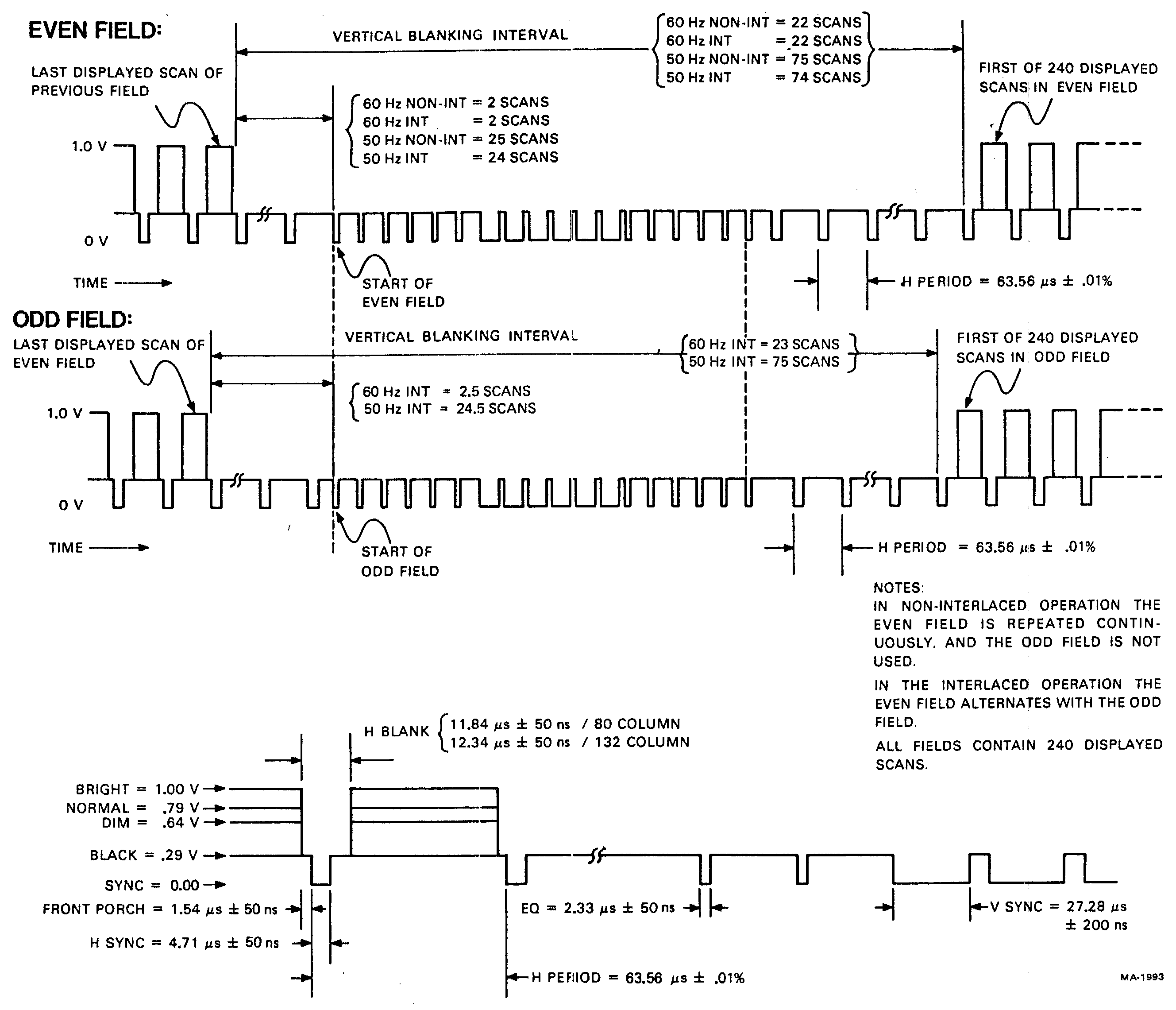
The composite video output provides RS170 output generated by combining the video signal with a composite sync signal. The output contains all video data appearing on the VT100 screen except that video which comes from J8. The output has the following nominal characteristics (Figure 3-4):
The composite sync waveform conforms to EIA RS 170 standards. The vertical interval is composed of six equalizing pulses, six vertical sync pulses, and six more equalizing pulses. The timing is as follows:
| Equalizing pulse width | = | 2.33 µs ± 50 ns |
| Vertical pulse width | = | 27.28 µs ± 200 ns |
| Horizontal pulse width | = | 4.71 µs ± 50 ns |
| Horizontal blank width | = | 11.84 µs ± 50 ns/80 column mode |
| = | 12.34 µs ± 50 ns/132 column mode | |
| Front porch | = | 1.54 µs ± 50 ns. |

An analog signal applied to the video input is “ORed” with the internal video signal such that the beam intensity at any point on the screen corresponds to the intensity of that signal which tends to make the beam brighter at that point. A video signal on this input affects only the internal screen and does not appear on the composite video output. This input has the following nominal characteristics:
The external video source must be synchronized to the VT100; it may do this by referencing the composite sync on the composite video output. This means that the VT100 video input will not synchronize with any composite video source including the composite video output of another VT100.